The previous tutorial is here:
Elbert V2 Not Gate Tutorial
Here is how to implement a 6 input Nand gate using the schematic input section of the IDE. Not sure why anyone would need a 6 input Nand gate but anyway...
Load up the project navigator by double clicking on ISE Design 14.7 icon:

Start a new project by clicking on the file menu and selecting new project.
The following window will be displayed:

Choose a suitable folder to store your project and select 'schematic' as the source type. We are going to use the schematic entry system to design our Nand gate. Click 'Next' to continue:
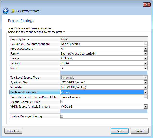
Enter the details specific to the Elbert V2 FPGA development board, make sure all of the details shown above are correct. We will be using verilog to implement the design. Click 'Next' to continue:
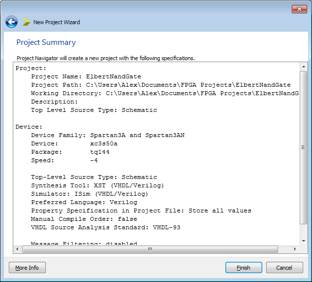
The project summary is displayed next - click finish to return to the main part of the IDE:
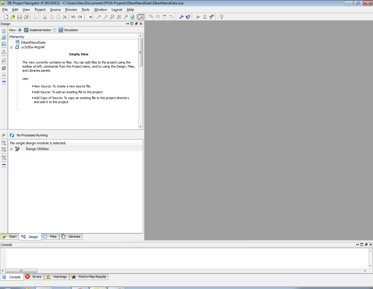
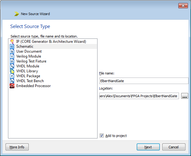
Right click on the 'Hierarchy' Section and add a new source file, select Schematic and give it a suitable file name:
Click 'Next' and a summary window will be displayed:
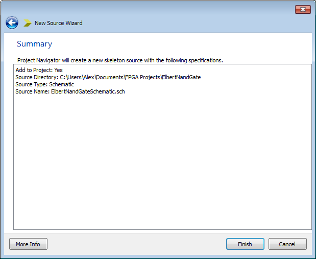
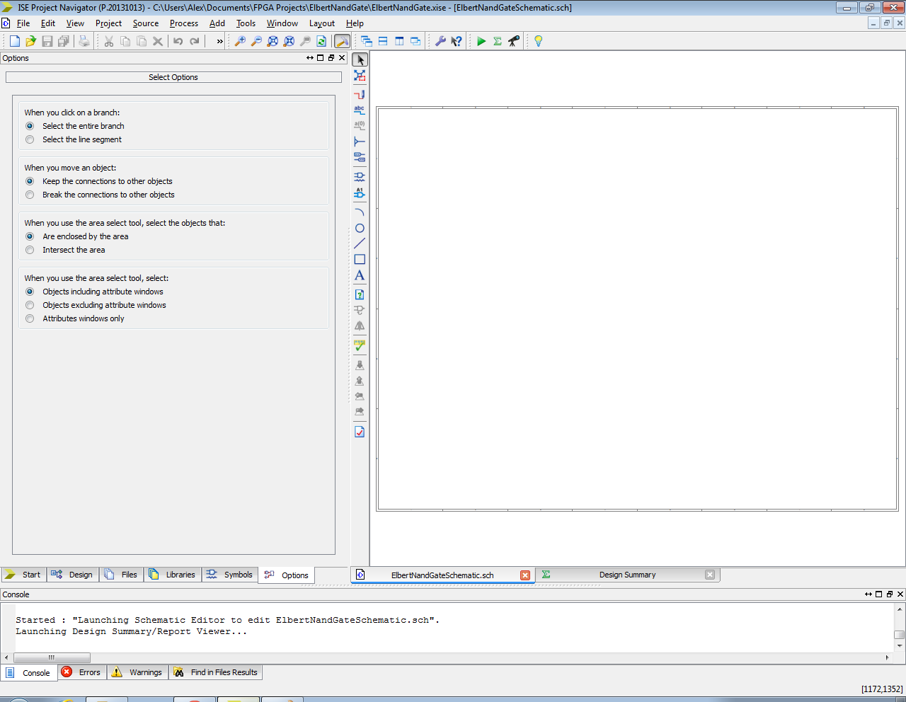
Click 'Finish' when ready to continue. After a few moments the Schematic Editor Screen will be displayed:
Zoom in a little by clicking on the 'magnifying glass icon' on the top toolbar:

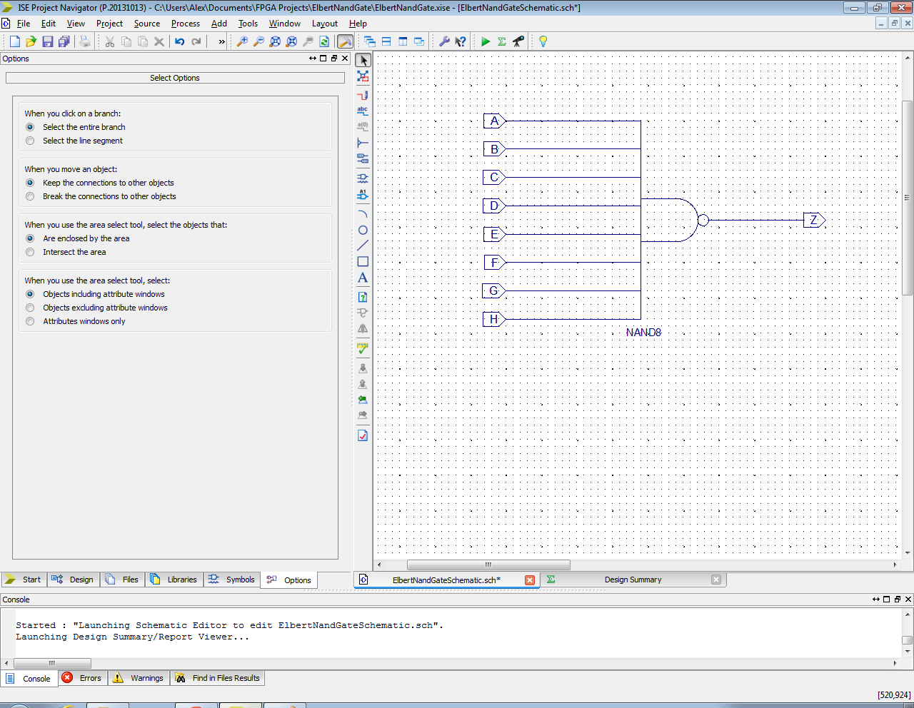
Next click on the add parts icon and then select logic for the category and Nand8 for the symbol. Then place the symbol on the design screen:

Add wires to the inputs and the output of the Nand Gate:

Add the wires by left clicking on the gate wire and then drawing a short line before double clicking to end the wire:

Next Add I/O markers to the inputs and outputs using the add I/O marker icon:
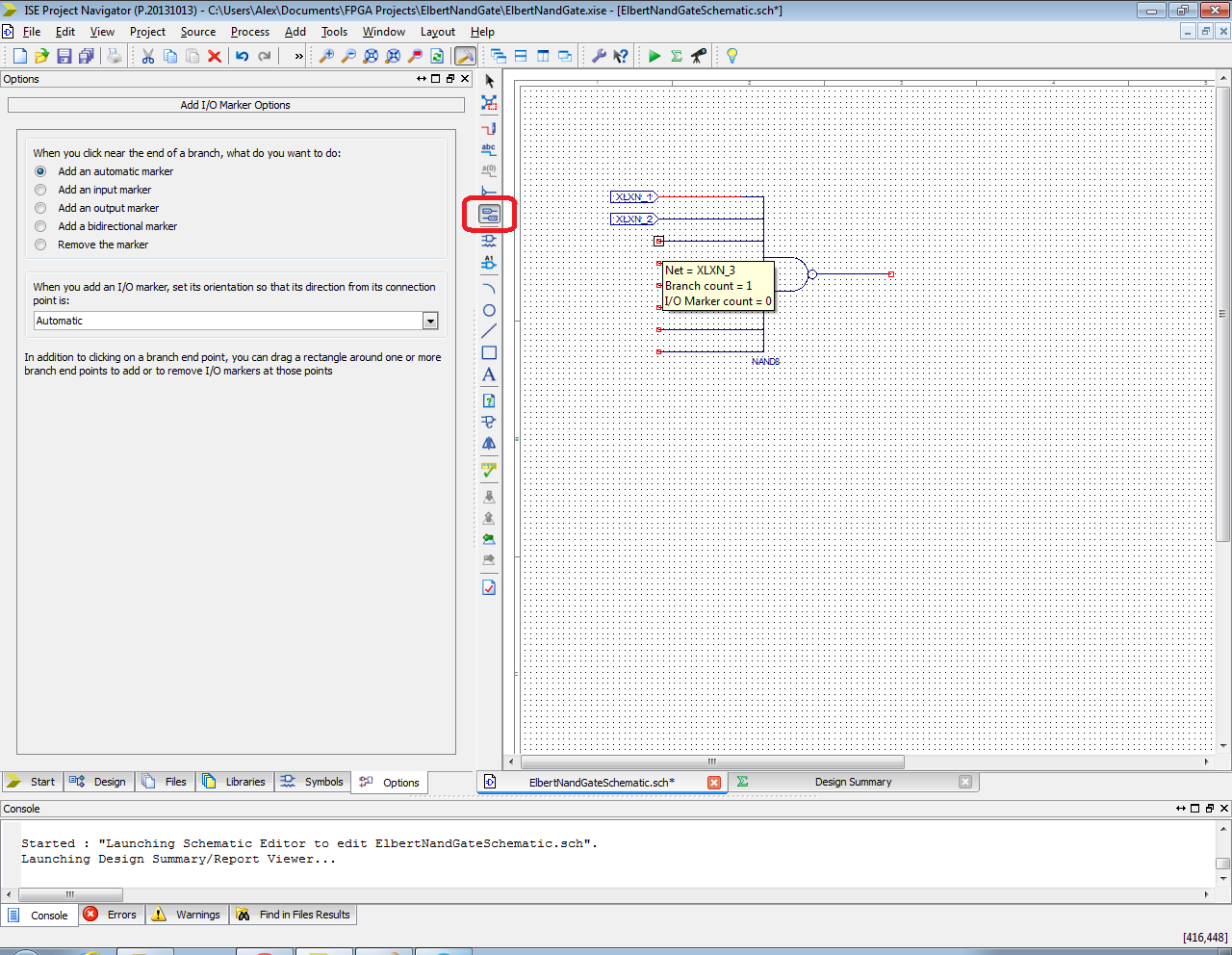
The diagram should now look like this:

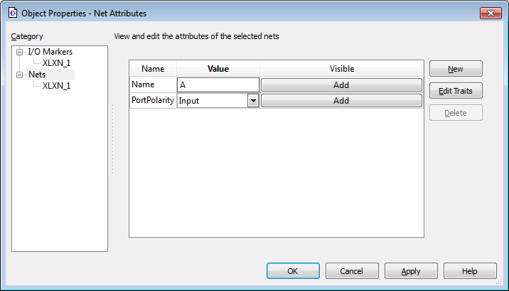
Double Click on the input arrow 'XLXN_1' - the following window will be displayed, change the name to 'A':
Repeat the process for all of the inputs and outputs - use sensible NET names, I used 'Z' for the output and 'A' to 'H' for the inputs. The diagram now looks like this:
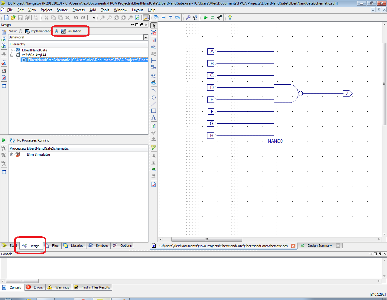
Click on the 'Design' tab in the bottom left corner of the screen and then select simulation:
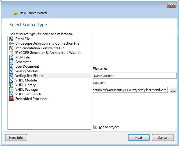
Right click on the 'Hierarchy' box and add new source file, select 'verilog test fixture' and give it a suitable file name:
Click 'Next' to continue, after a few moments the following screen will be displayed:
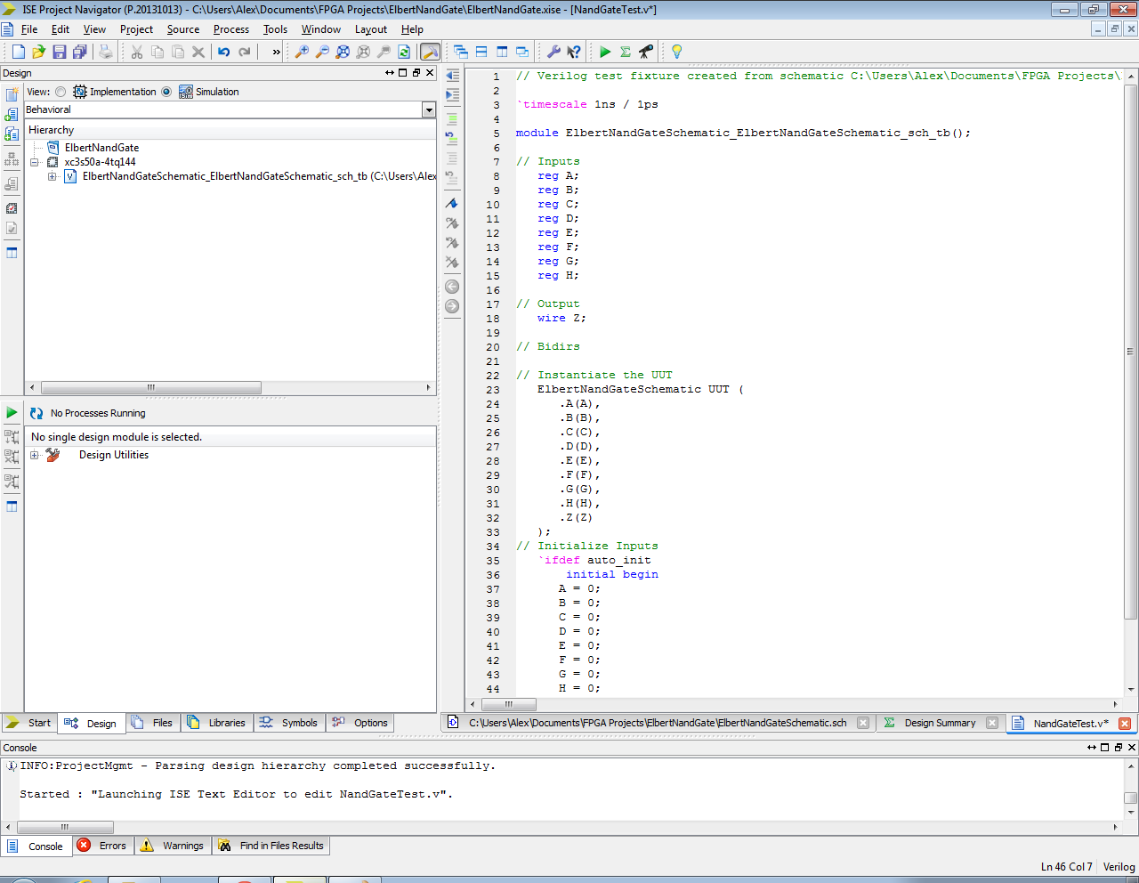
The IDE has helpfully created a test bench file based upon the information in the schematic. All we need to do is add some extra lines of code to test our implementation of an eight port Nand Gate:
// Initialize Inputs
initial begin
A = 0;
B = 0;
C = 0;
D = 0;
E = 0;
F = 0;
G = 0;
H = 0;
#10 // Wait ten nano seconds
A = 1; // Set the A input high
#10 // Wait ten nano seconds
B = 1; // Set the B input high
#10 // Wait ten nano seconds
C = 1; // Set the C input high
#10 // Wait ten nano seconds
D = 1; // Set the D input high
#10 // Wait ten nano seconds
E = 1; // Set the E input high
#10 // Wait ten nano seconds
F = 1; // Set the F input high
#10 // Wait ten nano seconds
G = 1; // Set the G input high
#10 // Wait ten nano seconds
H = 1; // Set the H input high
#10 // Wait ten nano seconds
#100 // Wait one hundred nano seconds
$finish; //finish the simulation
end
Remove the 'ifDef auto_init line and the 'endif lines and either copy and paste the above code or type it in....choice is yours. The screen should look similar to below:

Now is the time to save this file and then run a 'Behaviour check syntax' by right clicking on the 'Design Utilites' and choosing the appropriate option:

Once complete a green tick should be displayed as above. Now it's time to simulate the behavioural model - select that by right licking on 'Simulate Behavioural Model' After a few moments the following screen should be displayed:

Click on the 'Default.wcfg' tab to display the waveform from the simulation. It should look something similar to below:
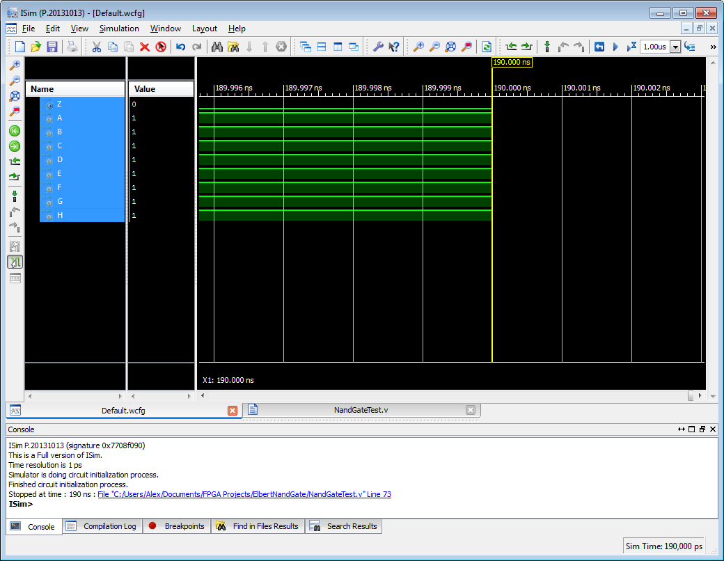
To expand the waveform and show the edge transitions click on the 'Zoom to full view' icon:

Now that we have proved our design will work it's time to tell the software which pins of the FPGA we would like to connect to the inputs and how we will display the output. First of all we need to remove the test bench file from the project as it isn't required for the implementation. Right click on the test bench file and remove it:

Then click on implementation and add a new source file - an 'Implementation Constraints file':

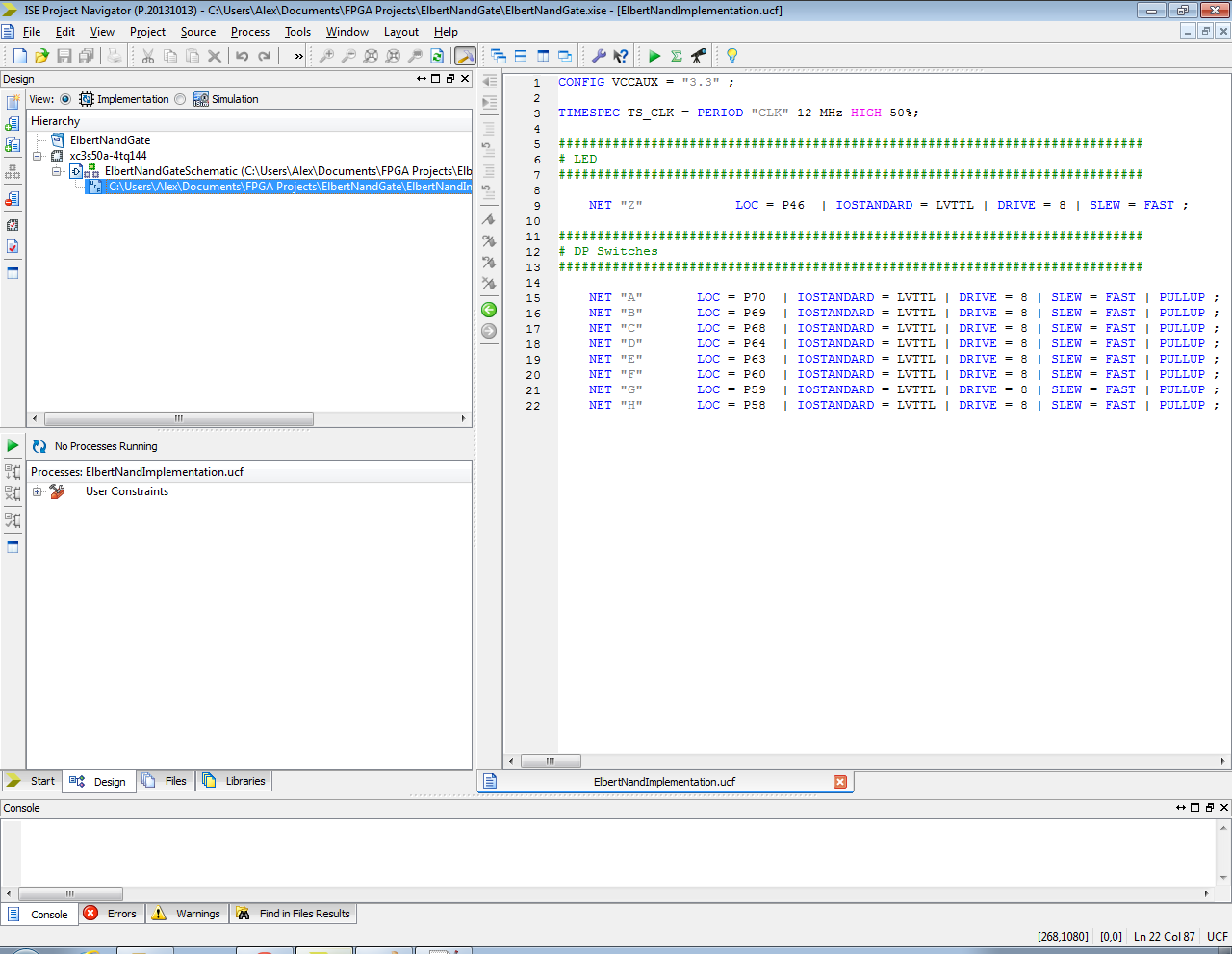
A new file will be opened inside the Xilinx IDE and it will be blank. We need to add the information required to tell the compiler which FPGA pins we would like to use as inputs and outputs. If we look at the Elbert V2 Schematic we can see that the development board has some DIP switches available to use as inputs and some LEDS available - lets use an LED for the output and the DIP switches as inputs:


We can see that LED 8 is connected to pin 46 and the DIP switches are connected from Pin 58 to pin Pin 70. Lets write the 'user constraints file':
CONFIG VCCAUX = "3.3" ;
TIMESPEC TS_CLK = PERIOD "CLK" 12 MHz HIGH 50%;
############################################################################
# LED
############################################################################
NET "Z" LOC = P46 | IOSTANDARD = LVTTL | DRIVE = 8 | SLEW = FAST ;
############################################################################
# DP Switches
############################################################################
NET "A" LOC = P70 | IOSTANDARD = LVTTL | DRIVE = 8 | SLEW = FAST | PULLUP ;
NET "B" LOC = P69 | IOSTANDARD = LVTTL | DRIVE = 8 | SLEW = FAST | PULLUP ;
NET "C" LOC = P68 | IOSTANDARD = LVTTL | DRIVE = 8 | SLEW = FAST | PULLUP ;
NET "D" LOC = P64 | IOSTANDARD = LVTTL | DRIVE = 8 | SLEW = FAST | PULLUP ;
NET "E" LOC = P63 | IOSTANDARD = LVTTL | DRIVE = 8 | SLEW = FAST | PULLUP ;
NET "F" LOC = P60 | IOSTANDARD = LVTTL | DRIVE = 8 | SLEW = FAST | PULLUP ;
NET "G" LOC = P59 | IOSTANDARD = LVTTL | DRIVE = 8 | SLEW = FAST | PULLUP ;
NET "H" LOC = P58 | IOSTANDARD = LVTTL | DRIVE = 8 | SLEW = FAST | PULLUP ;
Copy and paste the above code into the text editor and save the file:
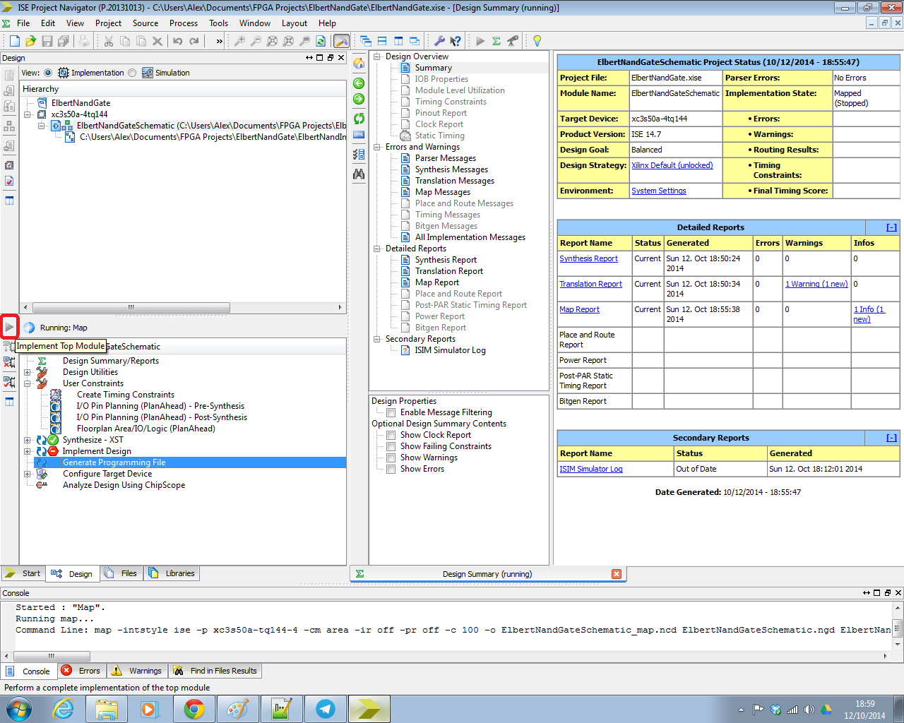
Now its time to generate the BIN file which will then be uploaded to the FPGA:
Right click on 'Generate programming file' in the processes section and check the 'Create Binary Configuration File':

Click on 'OK' to continue and then click on the 'Implement top module' button:
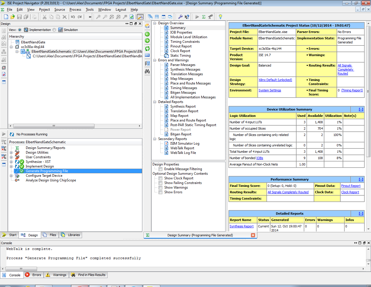
Once all the processes are complete you should be left with all green ticks - Synthesize, Implement Design and Generate Programming File:
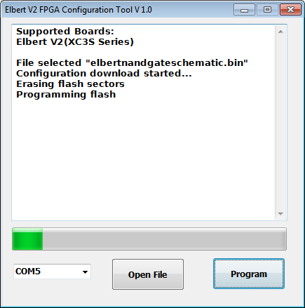
Now we can exit the Xilinx IDE and connect up the Elbert V2 Development board using a USB cable. Next load up the 'ElbertV2Config' program and choose the appropriate COM file for your Elbert V2 development board...mine is on COM5:

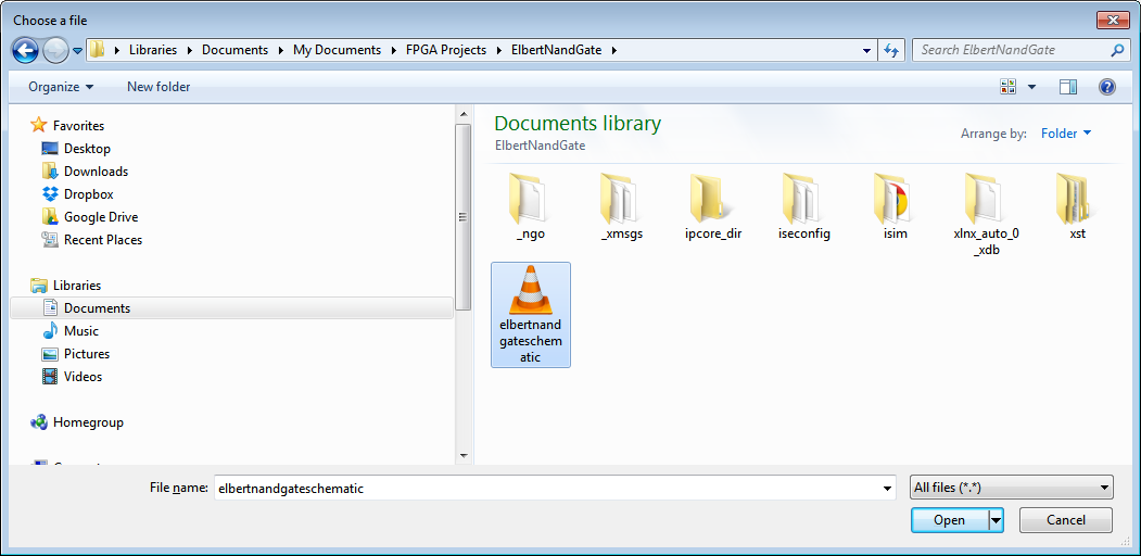
Click on the ' Open File' button and Navigate to the folder where the Nand gate project was stored. Locate the Binary file and select it:
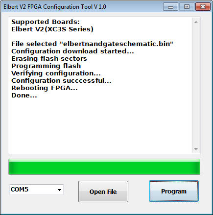
When ready click 'Program' and the FPGA will be programmed:
Once the programming has been completed the following will be displayed:
Now lets discuss NAND gate functions and what they do and how they work. A NAND gate is a logic function created in electronics. It is a shortened version of Not A and B. It means that an input A and an input B are 'anded' together and then the output is inverted. Information on Nand gates can be found here:
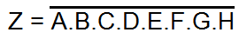
We have implemented an 8 input Nand Gate. If we had to draw a symbol it would look like this:

The boolean function is:
The truth table for this function would be:

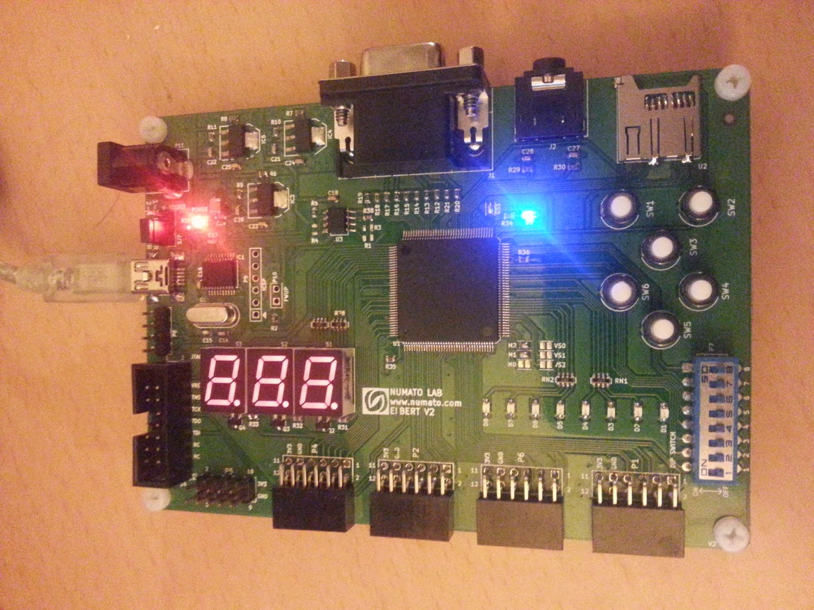
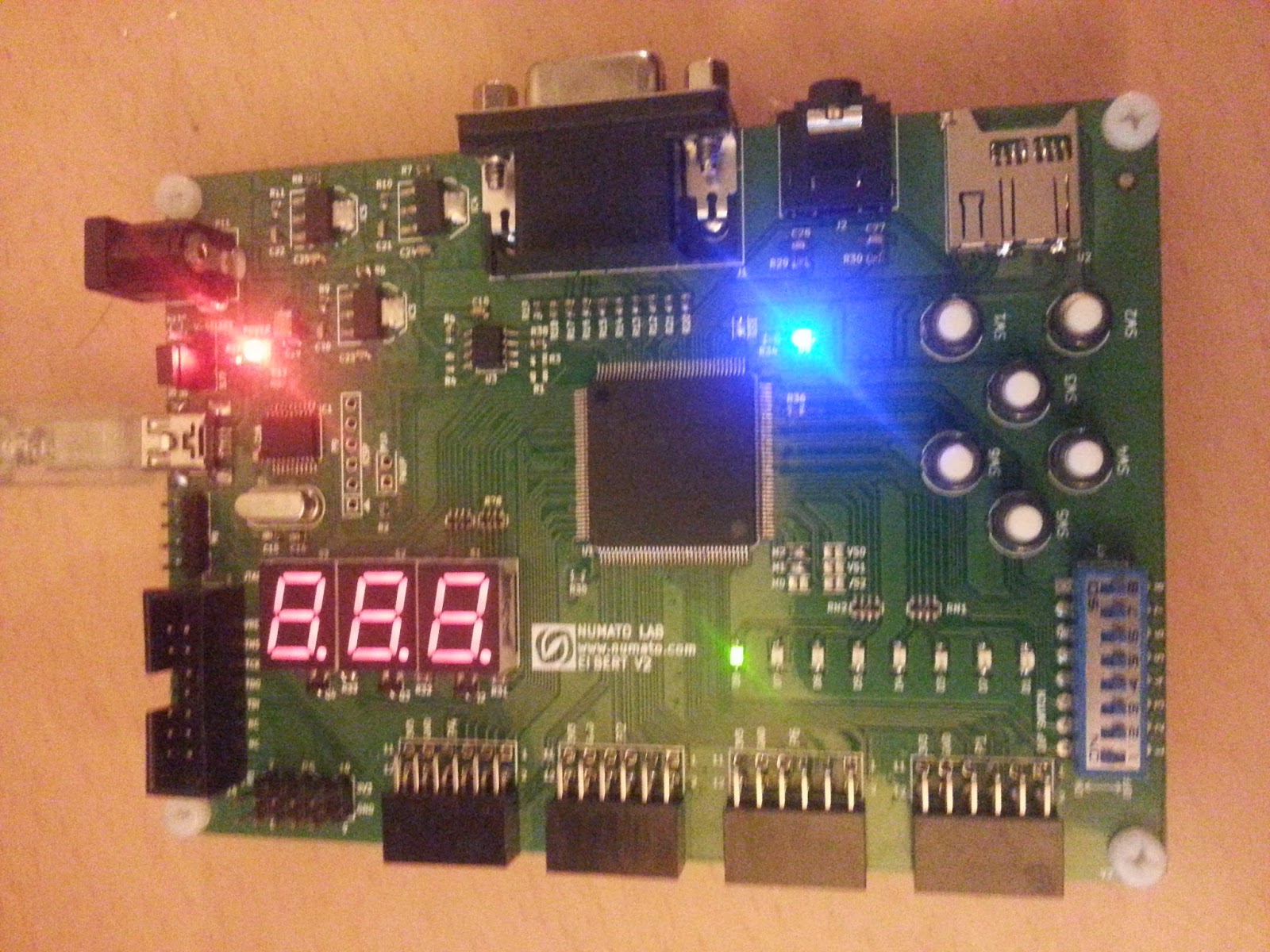
If we now look at the FPGA Development board and set the DIP switches appropriately we should see LED 8 light up:
If all of the switches are off - LED 8 is off:
But if any switch is ON then LED 8 lights up:
Here is a very short video showing the board in operation...no sound because there isn't much to say!
Thats all for now....take care - Langster
No comments :
Post a Comment