Spartan 3A Development Board - Numato Lab
FPGA stands for Field Programmable Gate Array - basically an integrated circuit where the function can be decided by the designer. Supposing a designer needed a circuit that would perform a specific boolean function continuously at very high speed. How could this be implemented? There are several options:
We could program a microcontroller to take perform the boolean function - possible but quite slow and time consuming...
We could create the boolean function in discrete logic - might take a very very long time and would be very difficult and expensive to implement...
We could write some VHDL or Verilog and program an FPGA - quite expensive and difficult to design but then this is not a simple problem...
A really good introduction to FPGA technology is here:
Embedded Micro - FPGA tutorials
I really want to get into FPGA technology because I can see it is useful...high speed instrumentation is difficult to achieve without being able to process data very quickly and something an FPGA can do very quickly (even faster than a microprocessor or controller) is process data!
There are other reasons for using an FPGA but my reasons are purely to learn the skill and to have some fun!
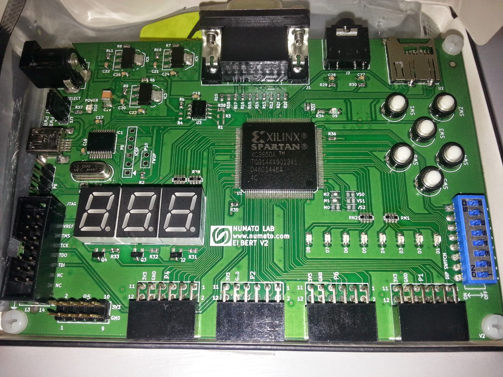
The development board I bought from India cost me £32 ($44) and I opted for it to be shipped by UPS and it arrived within three days! I got charged a brokerage fee by UPS so ended up paying an extra £20 in fees but this is still cheaper than a lot of the other options available.
Here are the specifications of the development board taken from the Numato Lab website:
- FPGA: Spartan XC3S50A in TQG144 package
- Flash memory: 16 Mb SPI flash memory (M25P16)
- USB 2.0 interface for On-board flash programming
- FPGA configuration via JTAG and USB
- 8 LEDs ,Six Push Buttons and 8 way DIP switch for user defined application
- VGA output
- Stereo audio out
- Micro SD Card Adapter
- Three Seven Segment Displays
- 39 IOs for user defined purposes
- On-board voltage regulators for single power rail operation
Exciting times! - I downloaded the USB driver, User constraints file and configuration downloaders from the Numato Lab website in preparation:
Download Elbert V2 files
I placed them in a Numator Labs folder on my Windows PC, and extracted the drivers and UCF file. Next I grabbed a USB A to Mini B cable and plugged it into the development board - The card powered up straight away and windows recognised a USB device had been attached. It tried to locate a driver and when it couldn't I navigated to the Numato Labs folder and pointed the driver installer to use the numatoCDC driver. It installed straight away and is displayed as a COM port in the device manager.

I then began to follow the instructions from the Numato Lab Website and their tutorials. The tutorials go through what an FPGA is and how it can be programmed and use a simple Not gate (inverter) example. When it comes to programming the device the tutorial refers to some Xilinx software which is needed to compile the example and generate what is called a 'Bit Stream'.
I went to the Xilinx website and tried to download the software suite known as ISE Webpack. In order to get access to the downloads section I needed to register with the site, obtain a licence file and then select the software package required. At first I downloaded the Vivado suite as this was the first and latest piece of software present in the downloads section of the Xilinx website download area. It was 6.7Gb of data! It took over an hour to fully download and turned out to not be what was required - the Spartan 3A device used on the Elbert V2 development board is not supported in the latest Xilinx design software - Very frustrating and confusing. I then spent a great deal of time reading the Elbert V2 manual and looking for the correct software and finally found it here:
Download ISE Webpack softare
It was also 6.7Gb in size and took a long time to download....I then proceeded to install the software and that also seemed to take a very long time to install! I then pointed the software to the location of the licence file and loaded up the software:
We are presented with the following user interface:
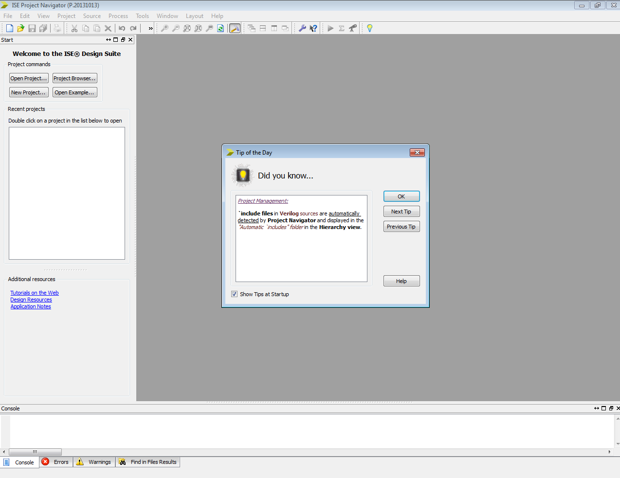
Get rid of the tip of the day box by clicking the OK button.
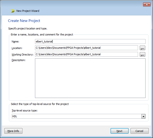
Next Click on the 'New Project' Button:

Choose a name for the project and choose to place the project in a suitable folder on your hard disk:
Click on the 'Next' button and fill in all the details as shown below - these are the parameters specific to the FPGA on the Elbert V2 Board - a Xilinx Spartan 3A - XC3S50A:

For this tutorial I will be using the Verilog style of programming for the FPGA. Verilog is a type of hardware description language. The other language often used is known as VHDL
Wikipedia Entry on Hardware Description Languages
Wikipedia Entry on Verilog
Anyway...as the original Elbert tutorial available discusses an inverter we are going to do the same thing. The tutorials from the Numato Lab website are here:
Numato Guide Part 1
Numato Guide Part 2
Numato Guide Part 3
Numato Guide Part 4
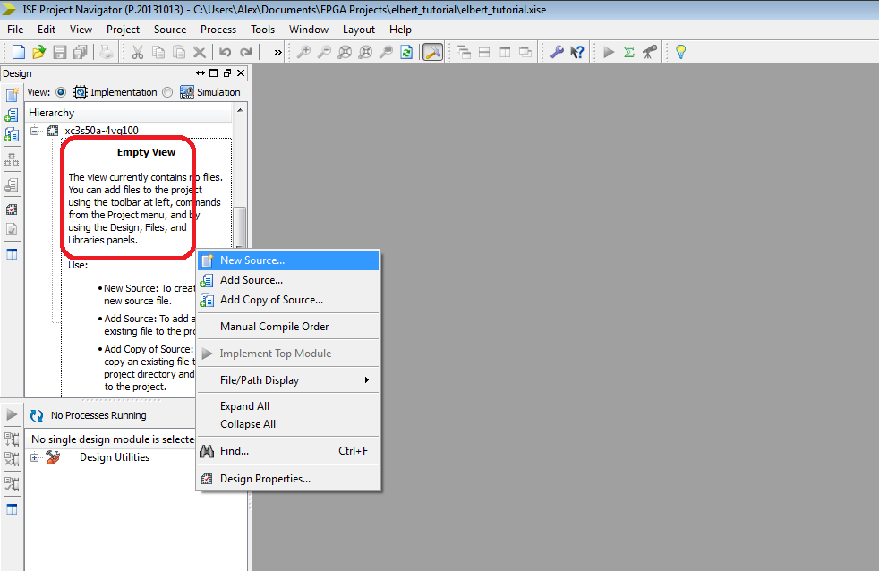
I am referring to them to write this tutorial...The webshots were different and it wasn't as straight forward for me as I think it could be...that's why I am writing this one - it will hopefully redress the balance a little. Click on the 'Next' button and you will be presented with the following window:

It confirms all of the details concerning the project - Click on the 'Finish' button to return to the main ISE Editor Screen:

Now we are going to create a text file which contains the Verilog code to model the function of an Inverter or NOT gate. Right click on the 'Hierachy' window indicated:
A new window will appear - select verilog module and type a suitable module name in the dialog box:

Click the 'Next' button and another window will appear - Fill in the details as shown below:
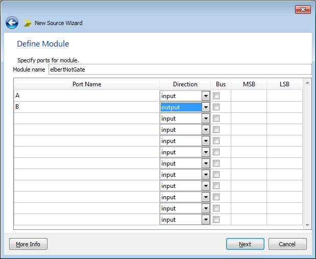
This means we are creating a verilog module which has one input ( A ) and one output ( B ) just like an inverter. This is confirmed in the summary window which is displayed when the 'Next' button is clicked on:

Click on the 'Finish' Button and you will return to the main ISE Webpack Screen. The source code file we just generated will be displayed:
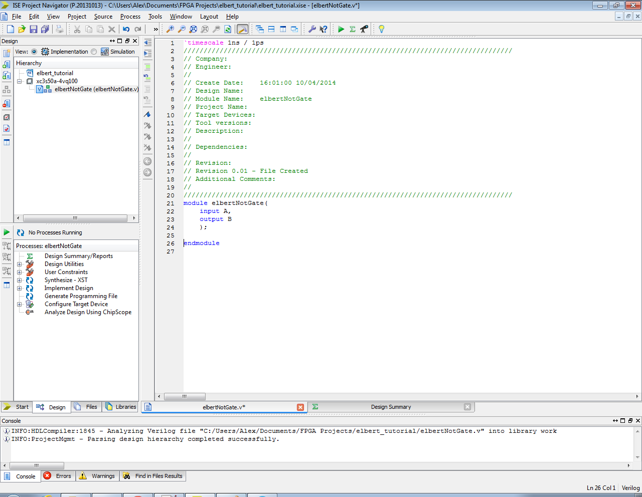
The screen to the right shows verilog module template with an input called 'A' and an output called 'B'. We now need to write the verilog code which models the behaviour of an Inverter or NOT gate:
On line 25 in the text editor (right side of the screen) type the following code:
input wire A;
output wire B;
assign B=!A;
Click on the Save button to save your work:
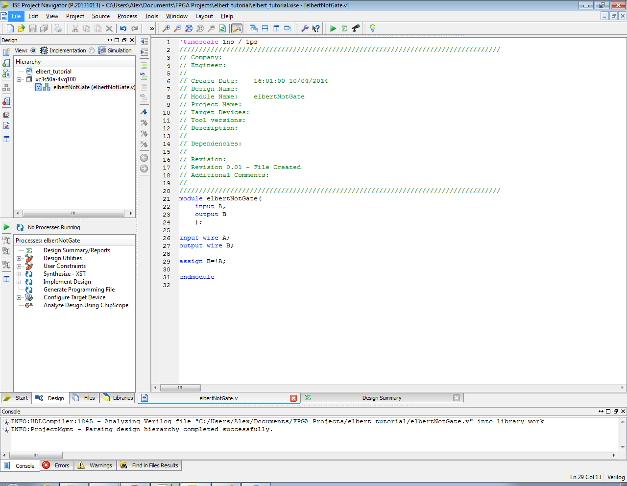
module elbertNotGate( // create a module called elbertNotGate
A, // It has one input called A
B // It has one output called B
);
input wire A; // The input A is a physical wired input
output wire B; // The input B is a physical wired output
assign B=!A; // Assign output B the inverse of input A
endmodule // End the module
Next lets check this code works properly by simulating it. This is an awesome feature of FPGA programming. Anything we type can be simulated to check it works properly! Right click on the Hierachy window again and 'add new source':

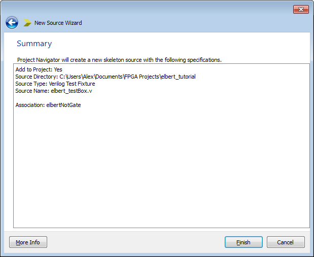
This time we are going to select 'Verilog Test Feature' and give it a suitable name:

Click on the 'Next' button and a new windows will be displayed:

Click on the 'Next' button to continue and a summary window will be displayed confirming the information we have provided for the test bench file:
Click on the finish button to continue and return the main ISE webpack screen. Now we need to enter some code which tells the simulator how to test the NOT gate module. Enter the following code after deleting the automatically generated code:
module elbert_testBox; // create a module called elbert_testBox
wire out; // create an output called wire
reg clock; // create a register called clock
always begin // Start the clock oscillating
#1 clock =!clock;
end
initial begin // Initialize clock at zero
clock = 0;
#10; // Wait 10 ns to end simulation
$finish;
end
elbertNotGate NotGate(clock, out); // Set the outputs
endmodule
Save the file and you should have the following on screen, also click on the simulate radio button above the hierachy box:
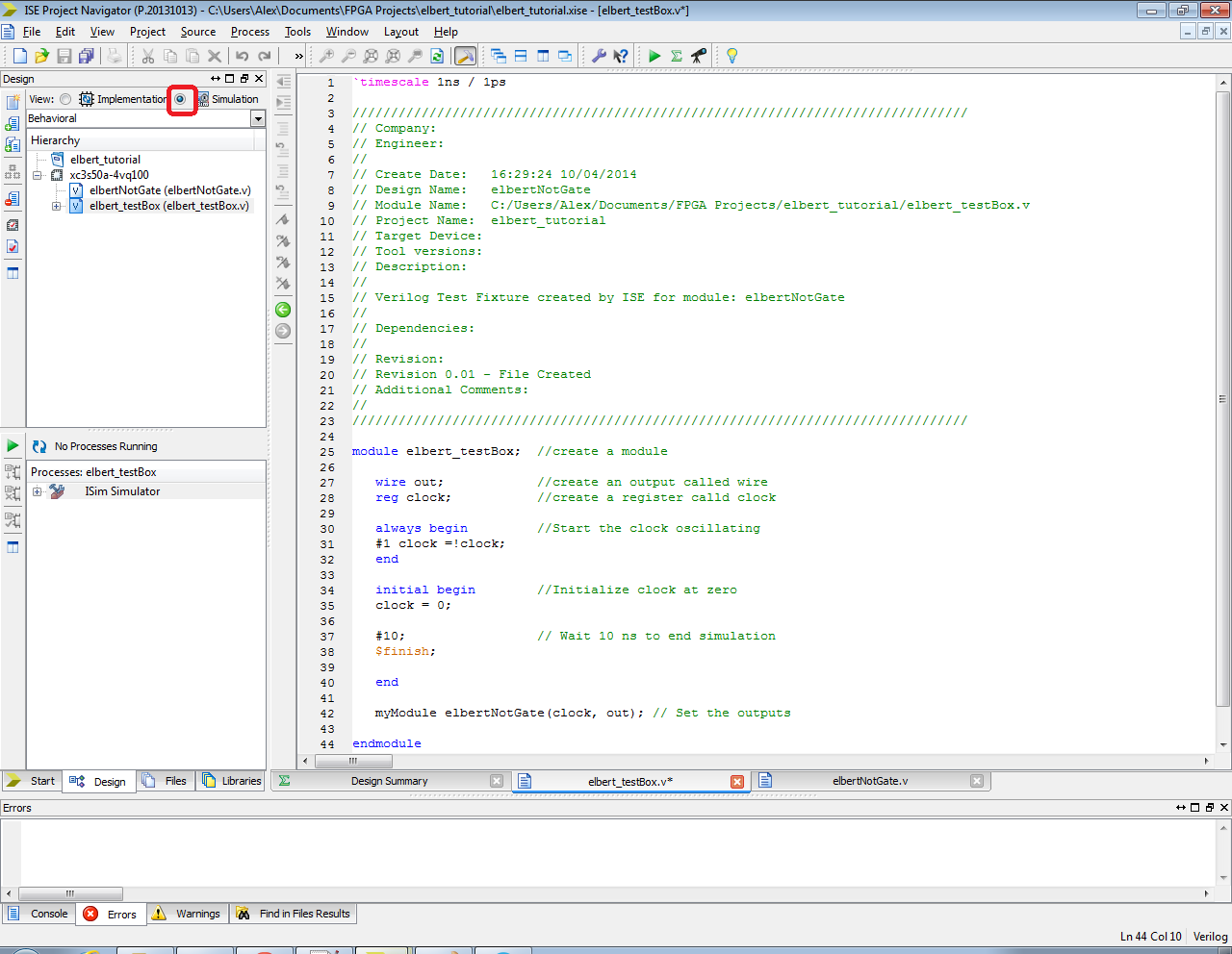
Now click on the newly created testbox module in the hierachy box, then select 'Simulate Behaviour Model' - right click on it and select 'Run'
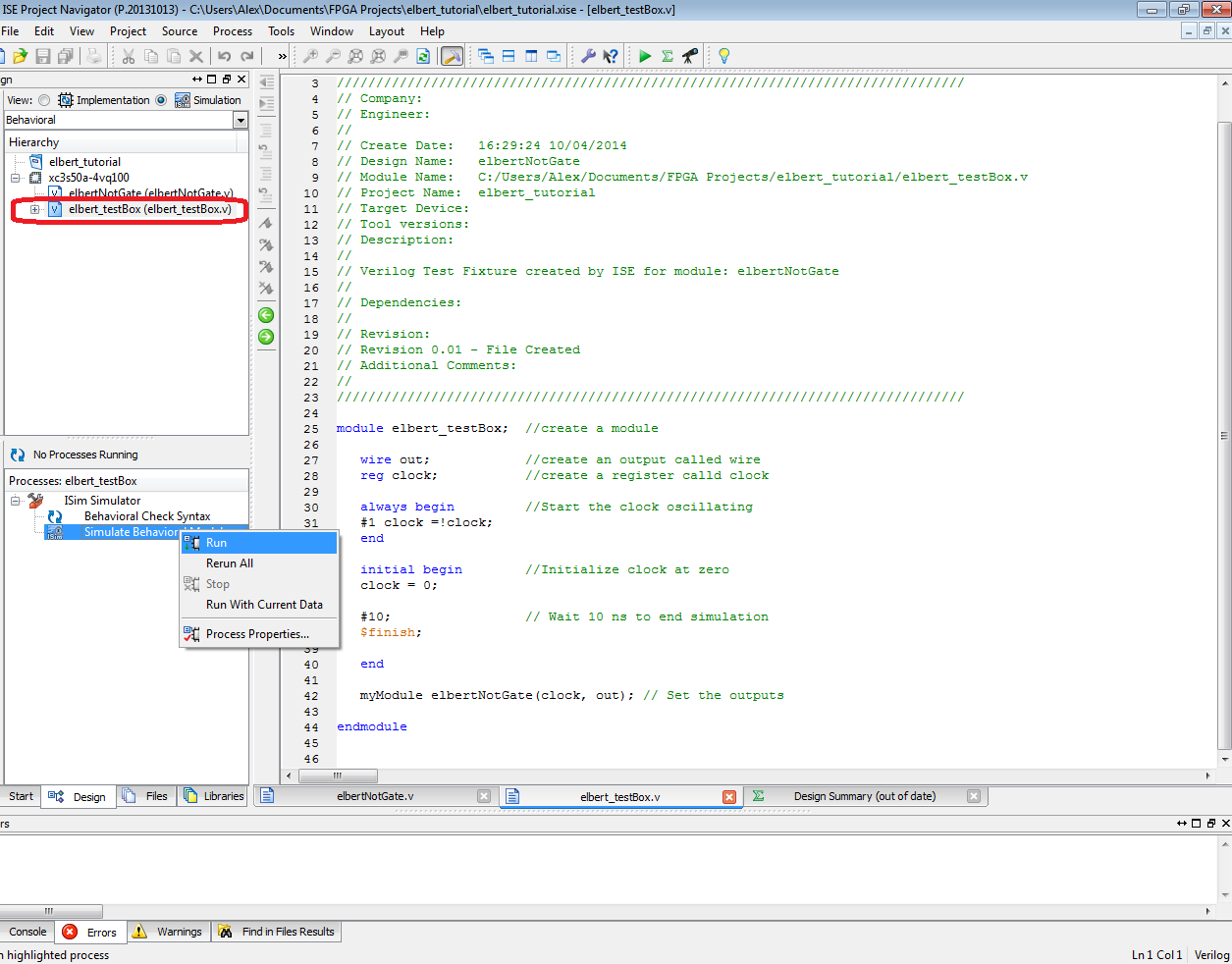
After a few moments (the software is processing the simulation) The following screen will be displayed from the simulation software module 'Isim':

Click on the Default.wcfg tab to display the results of the simulation:

Click on the 'Zoom to Full View' Icon on the top tool bar to display the waveform clearly:

It shows the operation of the Inverter. With a 1 nano-second clock input applied to the A pin the output is the inverted - Cool huh!
So....we have written a module in verilog that models the behaviour of an Inverter or NOT gate and we have simulated it. Now lets make it work for real <really big grin>
What we need to do is tell the Xilinx ISE Project Navigator software about the Elbert V2 development board - which pins are IO pins, which pins are connected to buttons, LEDS, audio output, microSD card and VGA connector etc. This performed using a text file called the user constraints file. We place the appropriate user constraints file in the project folder, tell ISE where it is and then when we come to compile the verilog code we can create a bit stream file which we then use to program the development board - a little involved but we will get there!
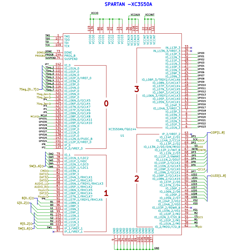
First off we need to know which pins are connected to what and in order to do that we need the schematic diagram for the Elbert V2 development board:
Elbert V2 Development board schematic
If you scroll through the pages eventually you will see the FPGA connections:
It's also a good idea to have a look at the Elbert V2 Manual:
Elbert V2 User Manual
On Page six it tells us how the LEDS and push button switches are connected:

So the push button switch 1 is connected to pin 80 on the FPGA and LED 8 is connected to pin 46. We can now use this information to generate a user constraints file:
# User Constraint File for NOT gate implementation on Elbert V2
# Push button switch 1 is connected to pin 80
#NET "Switch[1]" LOC = P80 | IOSTANDARD = LVTTL | DRIVE = 12 | SLEW = FAST | PULLUP ;
# LED 8 is connected to pin 46
#NET "LED[8]" LOC = P46 | IOSTANDARD = LVTTL | DRIVE = 12 | SLEW = FAST ;
We can change this information in the above text file to point to the variable names we used in our module - 'A' and 'B'
# User Constraint File for NOT gate implementation on Elbert V2
# Push button switch 1 is connected to pin 80
NET "A" LOC = P80;
# Push Button Switches.
# Internal pull-ups need to be enabled since
# there is no pull-up resistor available on board
NET "A" PULLUP;
# LED 8 is connected to pin 46
NET "B" LOC = P46;
All I have done is change the NET names to reflect the variable names we used in the module. I have also enabled the internal pullup resistor on pin 80 as without this the switch will not work - there are no external resistors connected to the switch.
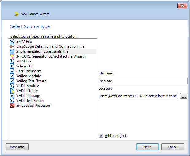
So now all we have to do is create this file in the project and add it - right click on the Hierachy window again and add an 'implementation constraints file':
Select the implementation constraints file:
Click 'Next' and the summary screen will be displayed:

Click on the 'Finish' button to return to the main screen next Click on the 'Files' tab in the bottom left corner of the screen:

Now double click on the notGate.ucf file to open it and then enter the UCF text for our project from above:

Click on the 'Design' tab in the bottom left corner and then select the implementation radio button:

If all goes well you will be presented with the following screen:
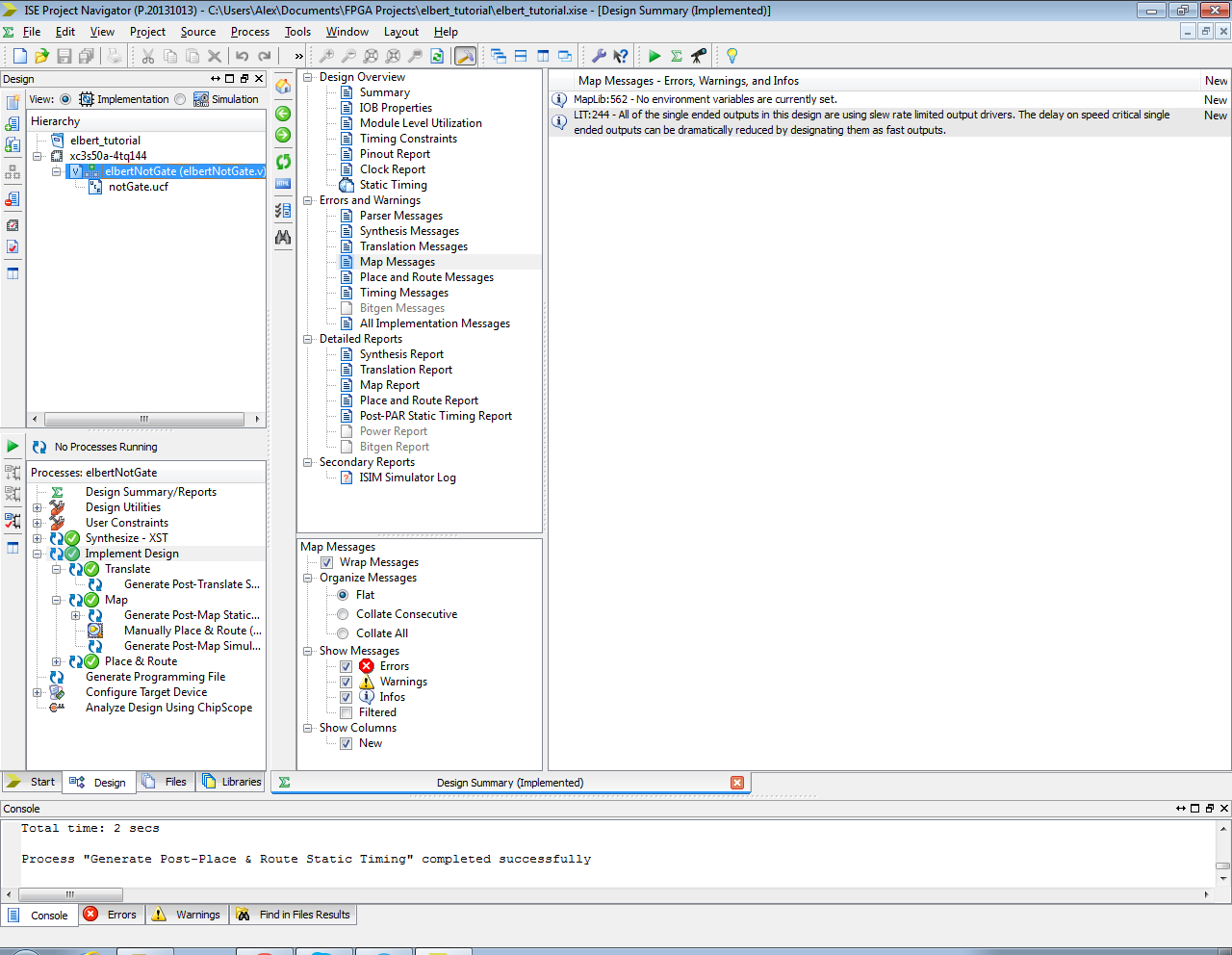
Now we need to generate a bitstream file to upload to the FPGA development board....right click on 'Generate Programming File' and select 'Run'

Once that is is complete and successful we need to load up the external programming software from Numato Labs called ElbertV2config - Elbert FPGA Configuration tool V1.0 and then select the COM port associated with the development board - mine was on COM 5. We then need to navigate to the project folder on the hard disk and select the binary file we just generated - elbertNotgate.bin
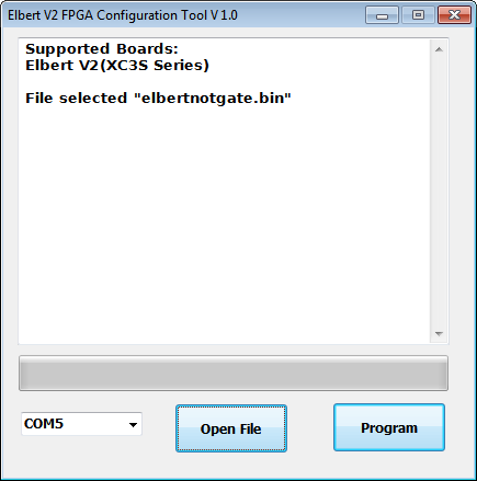
Click on the programming button when ready and then the bitstream file will be used to 'flash' the FPGA:

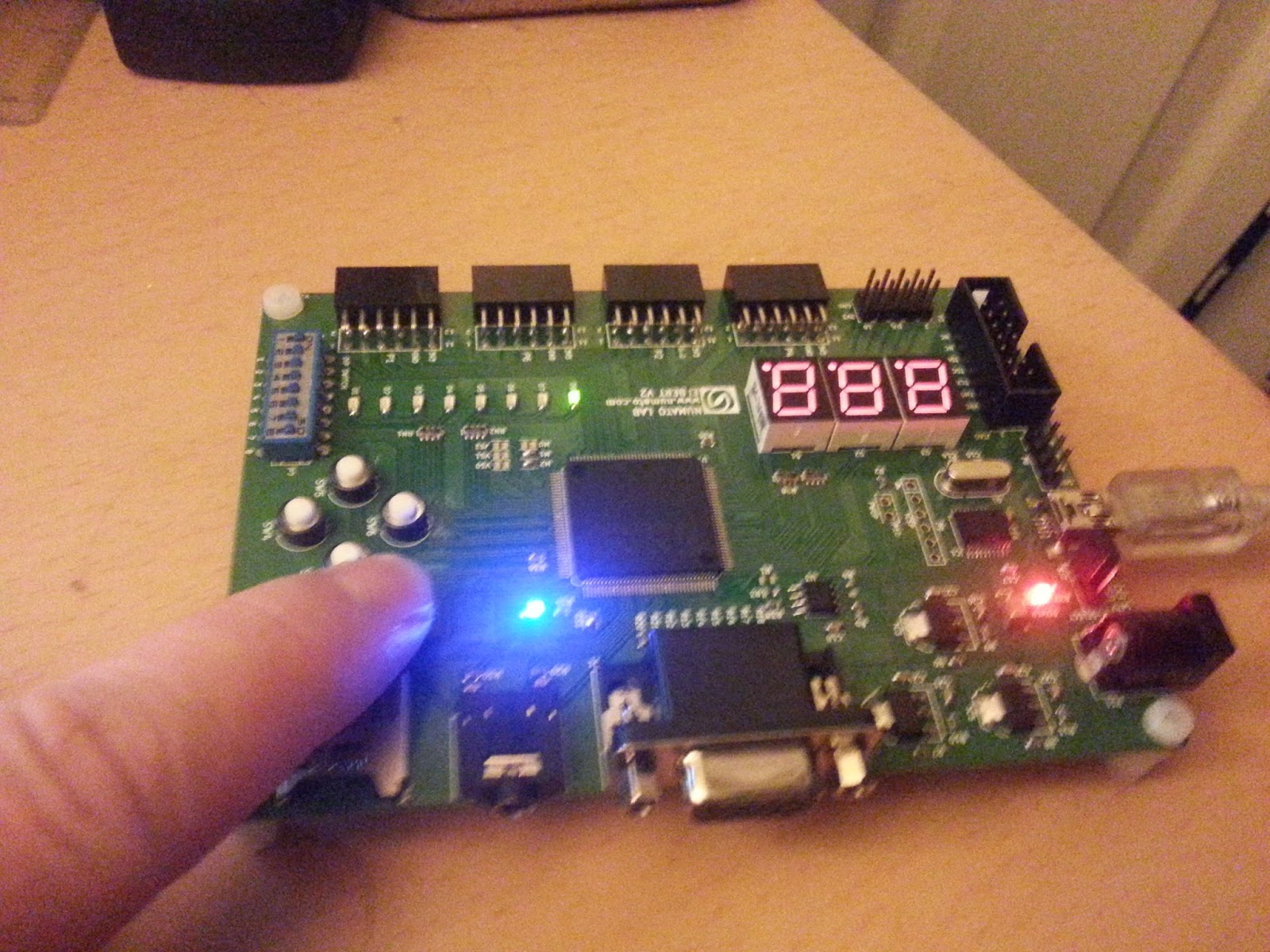
Once complete - advance to the FPGA development board and you should see that none of the LEDS are 'ON' and then when you press momentary button SW1....LED 8 comes on! Cool Huh! Well maybe not but its a start!
Here is a picture of the board and a short video showing the board working...take care people - Langster!
Thanks. awesome tutorial!
ReplyDelete