Saturday 16 July 2016

Switch De-bouncing in VHDL for the Mimas V2 FPGA Development Board

It's been a while since I blogged about my adventures in relearning VHDL.  I am slowly regaining the knowledge I used to have when I studied at University (That seems a very long time ago now). Slowly and steadily I'm building up the knowledge needed to use an FPGA for something useful.

I intend writing a couple of connected blog posts over the next week or so in order to demonstrate something more involved (and useful).

This post will concentrate on reading input from a momentary switch.  The Mimas V2 board has six momentary switches on the right side of the board below the micro-SD card slot.  Lets write some code which reads in one these switches with de-bounce code.  We can then use this code to implement a counter which we can display on the seven segment display.  The counter and the seven segment display section will be in later posts.  For now lets concentrate on reading in the switch properly.  For now we can display the output onto an LED

Mimas V2 Momentary Switches
Here is the general idea:
  1. Start
  2. User Presses a momentary switch.
  3. The FPGA reads in the button switch.
  4. The button read is de-bounced.
  5. The corresponding LED is illuminated until the button is released.
  6. Go back to step 1.
  7. End.
Lets fire up Xilinx WebISE and start a new project:


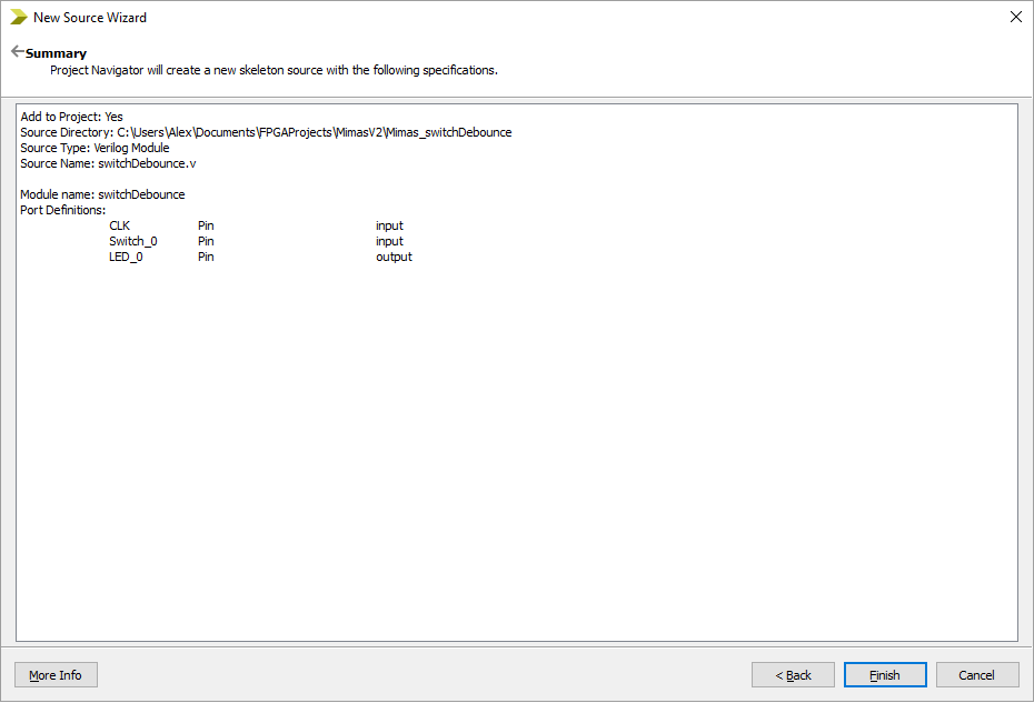
I called mine Mimas_switchDebounce - use any name you like!  Click next when ready:


Make sure all the above settings are entered so that the project is setup correctly for the Mimas V2. Click next when you are ready:


Click Finish to return to the main project screen.

Now left click on the project menu and select 'add new source':


In the dialog window that appears select VHDL Module and give it a suitable name - I called mine switchDebounce:


Click 'Next' when you are ready to continue:

We need to define the inputs and outputs for the debounce code.  We need to read in the raw button presses and then we need to display the results on an LED.  This all needs to be synchonised with the 100 MHz clock on the Mimas V2.  


Complete the form with the above settings and then click 'Next' to continue:


Click 'Finish' to return to the main project screen in WebISE:

Xilinx Webise has helpfully automatically generated some code for us....Let's examine the code.

LIBRARY IEEE; USE IEEE.STD_LOGIC_1164.ALL; ENTITY switchDebounce IS PORT ( CLK : IN STD_LOGIC; Switch_0 : IN STD_LOGIC; LED_0 : OUT STD_LOGIC ); END switchDebounce; ARCHITECTURE Behavioral OF switchDebounce IS BEGIN END Behavioral;

The entity statement defines the inputs and outputs to the FGPA - three standard logic pins, the switch input, the LED output and the 100 MHz system clock.

The architecture statement is where the 'behaviour' of the code will be defined.  There isn't anything in it yet but there will be!  Lets decide how we are going to achieve things.  There is more than one way of reading in buttons, checking that the button state has changed and then producing a result.

Lets make things easier for ourselves and draw a flow diagram:

This should make writing the code a little easier for us.  Every diamond is an if statement, every rectangle is a part of a process....simples!


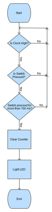
From the flow diagram we should be able to write the behavioural section of the code:

ARCHITECTURE Behavioral OF switchDebounce IS
SIGNAL inputFlipFlop : STD_LOGIC_VECTOR(1 DOWNTO 0); CONSTANT countMax : INTEGER := 100000000; SIGNAL count : INTEGER RANGE 0 TO countMax := 0; BEGIN PROCESS (clk) BEGIN IF (clk'EVENT AND clk = '1') THEN inputFlipFlop <= inputFlipFlop(0) & Switch_0; IF (inputFlipFlop(0) /= inputFlipFlop(1)) THEN count <= 0; ELSIF (count < countMax) THEN count <= count + 1; ELSE LED_0 <= inputFlipFlop(1); END IF; END IF; END PROCESS; END Behavioral;

Lets go though how the above code works:

SIGNAL inputFlipFlop : STD_LOGIC_VECTOR(1 DOWNTO 0); -- input flip flops CONSTANT countMax : INTEGER := 100000000; -- 100 MHz clock, delay is 100 ms and 100 ms = 10,0000000 ns SIGNAL count : INTEGER RANGE 0 TO countMax := 0;

The above lines create internal signals.  The first signal inputFlipFlop is a simple flip flop.  It is used to check if the button has been pressed or released (changed state).  The constant countMax is the delay period that is set to ensure that a button has actually been pressed.  It has been set to 100 ms although any number can be used.  It was calculated from the 100 MHz source clock.  1/100,000,000 = 1 ns and 10,000,000 ns is equivalent to 100 ms.  If a second was needed then the constant should be set to 1000000000 etc.  The signal count is the value of the number of clock pulses that has passed.  It is dynamically set to the maximum delay period set by countMax.

BEGIN PROCESS (clk) BEGIN IF (clk'EVENT AND clk = '1') THEN inputFlipFlop <= inputFlipFlop(0) & Switch_0; -- read the switch state IF (inputFlipFlop(0) /= inputFlipFlop(1)) THEN -- has flipflop changed state from previous state count <= 0; -- if flipflop has changed then reset count ELSIF (count < countMax) THEN -- if flipflop has changed is count less than countMax count <= count + 1; -- increment count by one ELSE -- count has reached countMax LED_0 <= inputFlipFlop(1); -- set LED_0 to the same state as the flip flop END IF; END IF; END PROCESS; END Behavioral;

The above lines perform the function that is required - the subject of the flow diagram:  
  • If the clock has changed state and is high then check if the flip flop has changed state.  
  • If the flip flop has changed state from it's previous state - This means a button has been pressed and if a button has been pressed then the count needs to be reset.  
  • If the count is less than the delay period then the count must be incremented.  
  • If the count has reached the delay period then the LED state needs to match the flip flop state.   
Here is the entire source code in case it's needed:

LIBRARY IEEE; USE IEEE.STD_LOGIC_1164.ALL; ENTITY switchDebounce IS PORT ( CLK : IN STD_LOGIC; Switch_0 : IN STD_LOGIC; LED_0 : OUT STD_LOGIC ); END switchDebounce;

ARCHITECTURE Behavioral OF switchDebounce IS
SIGNAL inputFlipFlop : STD_LOGIC_VECTOR(1 DOWNTO 0); CONSTANT countMax : INTEGER := 100000000; SIGNAL count : INTEGER RANGE 0 TO countMax := 0; BEGIN PROCESS (clk) BEGIN IF (clk'EVENT AND clk = '1') THEN inputFlipFlop <= inputFlipFlop(0) & Switch_0; IF (inputFlipFlop(0) /= inputFlipFlop(1)) THEN count <= 0; ELSIF (count < countMax) THEN count <= count + 1; ELSE LED_0 <= inputFlipFlop(1); END IF; END IF; END PROCESS; END Behavioral;

Save the file just in case - it's always a good idea to save your work!

Now we need to create an implementation constraints file to tell the system which pins are connected to the clock, switch and the LED.

Create an implementation constraints file using the same method used to create the VHDL source code.  Call it something sensible like switchDebounce.  Copy the code below into the file:

#+++++++++++++++++++++++++++++++++++++++++++++++++++++++++++++++++++++++++++++++++++++++++++++++++++++#
# This file is a .ucf for Mimas V2                                                                    #
# To use it in your project :                                                                         #
# * Remove or comment the lines corresponding to unused pins in the project                           #
# * Rename the used signals according to the your project                                             #
#+++++++++++++++++++++++++++++++++++++++++++++++++++++++++++++++++++++++++++++++++++++++++++++++++++++#

#*****************************************************************************************************#
#                                            UCF for MIMAS V2 Spartan 6 Development Board             #
#*****************************************************************************************************#

CONFIG VCCAUX = "3.3" ;

   NET "CLK"      LOC = V10 | IOSTANDARD = LVCMOS33 | PERIOD = 100MHz;

#######################################################################################################
#                                              Push Buttons Switches                                  #
####################################################################################################### 
    NET "Switch_0"           LOC = M18   | IOSTANDARD = LVCMOS33 | DRIVE = 8 | SLEW = FAST | PULLUP; 

#######################################################################################################
#                                                    LEDs                                             #
####################################################################################################### 
    NET "LED_0"              LOC = P15  | IOSTANDARD = LVCMOS33 | DRIVE = 8 | SLEW = FAST ;


Now it's time to 'compile' the code into a bit file and upload it to the Mimas V2:


Click on the green 'implement top module' arrow and wait for the code to compile.  There should not be any errors or warnings.

Now connect up the Mimas V2 board to your computer via a suitable USB cable and then fire up the Mimas V2 configuration tool.  If you are using Linux then use the appropriate python tool - I don't use linux often....only so much time to learn new things at the moment!  Select the appropriate COM port for your board and then navigate to the project...select the newly created bin file and click program!


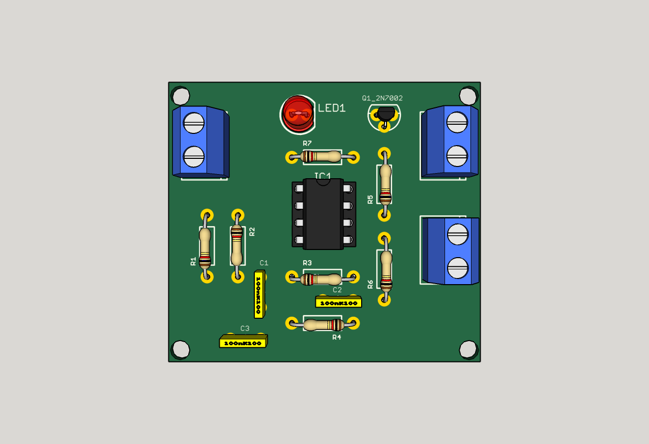
Once programming is complete you should see something similar to the following:


The more astute among us will notice that the LED starts high and is turned low when a button press is detected.  That is because the switches on the Mimas V2 board are active low....the code logic will need to be inverted in order to take the LED from low to high.  It's a simple enough edit.  We could also remove the seven segment display ghosting if needed...

That's all for now though people - more to come on this - next it's count the button press and display the result on the seven segment!

Hint change the line of code from LED_0 <= inputFlipFlop(1); to LED_0 <= not inputFlipFlop(1);


Wednesday 15 June 2016

Linux on the Mimas V2

Recently I found out it's possible to run an embedded version of linux on the Mimas V2 FPGA development board.  I'm not the best person at using linux but I did manage to get it working.

It is thanks to a lot of hard work that has been performed the people at J2-Open Processor:

http://j-core.org/

In order to make use of it you will probably need to update your Mimas V2 programmer firmware to work at 115200 baud.  This is so that the serial communications from the Linux core will work at a reasonable rate.

In order to achieve that you will need a micro-SD card capable of storing a small linux image.  Get hold of a micro-sd card and then download vmlinux from the link below:

http://j-core.org/#vmlinux

Copy the file onto the micro-SD card.  Do not try to write it as an image....its not like a raspberry Pi
( I may have made this mistake - thanks for the help Goran! )

Next you will need to update the programming firmware on your Mimas V2 to work at 115200 baud.
The firmware update increases the speed of communication between the PIC microcontroller and the FPGA device to 115200 Baud which is what is needed to upload programs from the arduino IDE.

You will need to download the following things in order to update the firmware:


Hex file to update baud rate to 115200

*Warning* There is currently no firmware to return the Mimas V2 PIC Microcontroller to it's original state and the updated firmware is currently beta only - it does have some issues. These are being addressed but at the moment there is currently no way to return the PIC on the Mimas V2 board to its factory settings.

I have not found any issues from doing this upgrade as yet however.

When my version of the Mimas V2 FPGA development arrived as new it did not have some header pins soldered into P3 - So I had to solder some in. This is needed to perform the PIC firmware upgrade:


Mimas V2 FPGA Development board without Firmware Upgrade Header

Here is my board with the header pins soldered in:


Next you will need to short the pins together to put the PIC Microcontroller into firmware upgrade mode:


Connect up the Mimas V2 FPGA development board to your computer - it's time to update the PIC firmware! When you connect up the FPGA development board windows will install a generic USB driver for the PIC device - this is meant to happen.

Open the folder where the software has been downloaded and execute up the firmware downloader program, Ignore the standard windows warning message - the program is fine. You should see something similar to the image below:


Click on 'Open Hex File' and navigate to where the 115200 baud update file was extracted - it's called MimasV2W@115200Beta.hex:


Click 'Open' to continue and then click on 'Program/Verify':


If all went according to plan you should see the above message!

Once that has been done you can remove the programming link.  Now it's time to upload the bin file to the FPGA which will create a soft processor which then accesses the micro-SD card and runs a version of Linux.

Now we need to download the file below - it's the bin file for the FPGA which runs at 115200 baud and adds the soft processor to the FPGA etc


Now upload it to the FPGA using the appropriate program - I don't use linux and so I use the MimasV2Config.exe program in Windows.  If you are using Linux then there are python scripts available.


Select the COM port associated with your Mimas V2 FPGA Development board - mine was COM 22:


Then click on 'Open File' and navigate to where the mimas_v2_115200.bin file is located:


Then Click program!


Once it has completed.  The FPGA will reboot and the seven segment display will go through a process.  At the end of the process it should look the like the picture below:


Next it is time to check all is working.  Move the programming direct switch SW7 over to the right - towards the VGA connector.  Then load up the serial terminal program of choice.  In my case I use RealTerm but in theory any serial terminal software 'should' work:

It is important to set the display to ANSI so ensure that spurious characters are not displayed.  In realTerm:


Then click on the port tab and set it to reflect the settings for the serial port on the Mimas:


Then when you are connected it should be possible to reboot the board by manipulating SW7:


Once it has completely booted the command line prompt should be displayed:


Type some commands in and check all is working!  I tried LS and DMESG etc.  All seemed to respond correctly.  I should be honest here and explain that my Linux skills are not as strong as they could be.  I use it when necessary.  I have only so much time and brain space available these days. When I have to learn something I do...I haven't 'had' to learn Linux command line stuff much yet!


I think to properly make use of this the Mimas V2 needs an Ethernet port.  Something I was thinking of designing although I may try and cobble something together from a breakout module.  There are lots available to try.

That's all for now - take care - Langster!

Thursday 9 June 2016

Designing a pressure sensor using Velostat


In the previous post I designed a circuit which was supposed to read in when pressure was applied to a custom sensor made from velostat.

The first post on the Piano conversion

I made a sensor out of some single sided FR4 printed circuit board material, some foam tape, two pieces of wire, a small 1 cm x 1 cm piece of velostat and some sticky tape!

Custom Pressure Sensor using Velostat
This is just a prototype and may not be my final version of the sensor. I wanted to see how well velostat worked and how it would behave. It seems to work really well!

I found from measurements with my multimeter that when the pressure sensor is not touched the resistance across the wires is 30 kΩ. When pressure is applied it drops to 1 kΩ. That should be more than good enough for the purposes of detecting a key-press!

The constructed pressure sensor
Next the PCB designed in the previous post was etched, drilled and populated. It etched well and I populated it with the designed components:

The Underside of the PCB 
The topside of the PCB with components

I then wrote some quick test code for the arduino because I'm leaning towards using an arduino for the microcontroller:

/*
Pressure Sensor test Code
For Electronic Piano
(c) A. Lang 2016
 
*/

// These constants won't change.  They're used to give names
// to the pins used:
const int analogInPin = A0;  // Pressure Sensor connected to A0

int sensorValue = 0;        // value read from the pressure sensor via the amplifier stage
float outputValue = 0;      // value output to the Serial port

void setup() {
  // initialize serial communications at 9600 bps:
  Serial.begin(9600); 
}

void loop() {
  // read the analog in value:
  sensorValue = analogRead(analogInPin);            

  // print the results to the serial monitor:
  Serial.print("sensor = " );                       
  Serial.print(sensorValue); 
  Serial.println();
       
  // wait 10 milliseconds before the next loop
  // for the analog-to-digital converter to settle
  // after the last reading:
  delay(10);                     
}
The code is very similar to code I had written before - what is it with me and pressure sensors at the moment! I then uploaded the code to the arduino and tested it - It didn't work as planned - I may have been a little disappointed at this point....

I then thought about my circuit and looked at the schematic:

The original Key Press schematic

I realised I had made a mistake. I didn't account for how the velostat would behave in terms of it's resistance. I thought it would have a resistance of around 1 kΩ and vary....it doesn't it's resistance is 
30 kΩ and varies down from that when pressure is applied. Because of this I need to tweak my circuit from behaving as a two stage buffer to a simple analogue comparator and buffer. Luckily it won't be too hard to change things!

Here is the new circuit:

Add caption
The Key Press Schematic Version 2 

The new circuits works in a similar fashion as the previous one. The velostat pressure sensor makes up a voltage divider. The output of the voltage divider is connected to an analogue comparator made with the first op-amp in an LM358 dual op-amp IC. The negative input has a 2.75 V reference set by the 8.2 kΩ resistor and the 10 kΩ resistor. The output of the 1st op-amp is then connected to a buffer amplifier with a gain of two and then the output is connected to a FET and an LED. The output will be sent to the ADC of the micro-controller which will probably be an Arduino.

To test the circuit I removed a 10 kΩ resistor and then added a 7.5 kΩ resistor (because I couldn't find an 8.2 kΩ resistor). Here is a photo of the modification:


Here is the modified PCB layout although I probably won't etch this board again. I'm going to re-design it to use surface mount components and be a smaller form factor. It would be nice if each board fit snugly under each piano key.

The New Key Press Layout
I then connected the circuit back up to the arduino and pressed the sensor! It worked. The LED lit up - although I wish I had used a brighter LED...but SUCCESS!! So sweet...


Here is a graph I made from the serial monitor results. It looks very similar to the simulated oscilloscope trace from the first post!
The results from the serial monitor
So now we have a valid method of reading key presses we need to scale things up - and shrink a few things down. I will redesign the key press PCB layout to use surface mount components to take up as little room as possible. Then we need to look at multiplexing all of the signals together...and for that I'm going to use the 74HC4076 integrated circuit breakout board.

That's all for now people - take care!

Sunday 5 June 2016

Converting an upright piano to an electronic midi piano

The Manchester Hackspace has recently moved.  When the move occurred there were two old upright piano fortes found in the corner of the new place...I asked to keep them!  I have been meaning to attempt a conversion from an acoustic mechanical piano to an electronic one for a very long time. Tuning my old walnut cased iron framed piano is becoming too difficult.  I miss being able to play in tune and with other instruments.  I also seriously miss being able to compose music and I used to use midi extensively to achieve that.  I haven't the space to write, play and record every instrument....so instead I used to use midi software on an external computer and have that record, notate and sequence the different parts to make create my opus!  Years ago I had access to an Atari ST 520FM which had built in midi ports - it made this very easy, I also had access to a Clavinova CLP-360 Yamaha electronic piano.  It was awesome and I miss it dearly...

So rather than let my creative talents go to waste I plan on tuning one of the pianos up as much as possible and restoring it to as near working condition as possible.  This can then be kept for posterity or donated to a worthy cause...It was looking a little shabby when I found it but I have cleaned it up and opened up the panels:

Here are some photos of the piano:

A classic Upright Piano with the covers off!

The iron frame and the strings

The pedals, the sustain has definitely seem some action!

Another side shot of the slightly...better piano!

There are actually two pianos physically they look very similar but one was in much better shape than the other.  Here is a video of the better one...One of the D flat keys does not have a bridal strap and so won't play or return.  I'm going to replace that strap but other than that it's got a nice action and is very easy to play...better than my own!  It was however horribly out of tune...


I have a piano tuning kit I bought off ebay for doing my own tuning so I broke it out and set to it. Tuning a piano is an art...it's difficult and takes skill and practice.  I did get it mostly in tune, some of the higher and lower notes beat me and I will spend a bit more time on it.  I am jealous of how easily played this piano is...my own keys are much stiffer and harder to play...mine also is in B flat...this piano tuned to A (440 Hz) without too much issue.

Here is the piano now tuned...hopefully it sounds better! EDIT - I haven't got a video of the tuned piano to share yet - I will upload one soon.  The internet needs more of my poor piano playing skills shared!


The plan with other piano is to remove the hammer action and strings and place some sensors underneath the keys. The sensors will connect to a microcontroller which will then send out midi data which can be used to drive a midi based synthesizer which will in turn be connected to an audio amplifier and a couple of speakers mounted inside the cabinet. The benefits of doing this are:

  • The piano will always be in tune!
  • A midi synthesizer can produce thousands of different voices - a whole orchestra and more!
  • The piano can be used as a midi Jukebox and a band in the box.
  • It is a great excuse to investigate touch pressure sensor technology.

Here is the current plan in a diagram


There are many aspects and parts to the project which will need careful thought and consideration.  I don't want to lose the piano's playability. If I remove the action - the mechanical part of the piano which converts the key press to strike a note the piano won't play as well. Here is a video I found on youtube which shows how a piano key functions:


I think in order to make this work it will be necessary to add a spring mechanism to where the key would normally pivot the action mechanism to get the key to return to it's original position. I am not great at mechanical engineering - here is my chance to improve!

It will also be necessary to sense the note being played. Most electronic pianos have a maximum number of keys being able to be played at the same time - this is known as polyphony.

An explanation on Note Polyphony

It would be nice to be able have at least a 32 note polyphony without any noticeable lag or delay. I'm not going to be playing pieces like this but being able to play 32 notes a once puts this device in the category of a reasonable electronic piano.

https://en.wikipedia.org/wiki/Two_hundred_fifty-sixth_note

So lets recap the requirements of the input section:

  • Sense at least 32 simultaneous key presses
  • record how long each note was held for 
  • record how hard the note was pressed

To do this we will need a pressure sensor which can easily be built and placed underneath the key of the piano.

I recently took some inspiration from this project:

http://liamtmlacey.com/vintage-toy-synthesiser

Liam used a sensor material known a velostat. It is a very interesting material which converts pressure into an electrical signal - it's electrical resistance changes as pressure is applied. I bought some from Proto-Pic

Velostat from Proto-pic

My plan is to combine the velostat into a simple resistive divider circuit which is then connected to the analogue input of a microcontroller and use this to 'sense' the note or notes being played.

A piano has 88 keys! If we want to sense them being played we need a way of reading in 88 analogue inputs. An arduino has six analogue inputs....an arduino mega has a few more but still not enough! We could use multiple microcontrollers but that makes things awkward and expensive as we need to then to synchronize them all...yikes!

I think this will require some analogue multiplexing in order to work well and not be overly cumbersome....I looked at a couple of the analogue multiplexers available and settled on this one:

74HCT4067 - Analogue Multiplexer

It's basically a single throw sixteen throw switch which can be controlled by a microcontroller. There lots of breakout boards available on the internet. I bought this one:

Ebay shop - 74HC4067 breakout board

I haven't used it yet....my first plan is to test and model the analogue input stage...then connect it to the multiplexer and then use that to scale up for 88 keys.

In order to make this work we will need a lot of multiplexers:

88 keys / 16 channels = Number of multiplexer devices needed

therefore 5.5 devices (six) in reality.

Before that we need to make a sensor measurement stage.  I've decided to use a buffered simple resistive divider circuit:

The Sensor Measurement Stage
The above circuit is an approximation of how the electronics will read a key press.  The circuit functions as follows:

The momentary switch and the 10 kΩ potentiometer model the behaviour of the velostat material. I don't have much information on the resistivity of the velostat but I have tried it and I do know that it's resistance does vary with pressure - I measured it with a multimeter. The resistor R1 makes up a voltage divider circuit. When the piano key is pressed the resistance of the velostat changes which is detected by the LM358 Op-Amp. The resistor R5 and the capacitor C1 make up a low pass filter. It might not be necessary but I'm trying to ensure that no external electronic noise is presented to the op-amp. I only want to measure key presses, nothing else. The first op-amp is configured as a non-inverting amplifier with a gain of two. The 100 pF capacitor limits the bandwidth of the op-amp restricting it's operation to low frequencies, another way to limit noise being passed on to other parts of the circuit. The second op-amp stage is again a simple non-inverting op-amp stage with a gain of two. The output signal presented to the next stage will be between zero and three and a half volts. That should be more than enough range present to detect key presses with good sensitivity. The output will be connected to an analogue to digital converter which will probably be a ten bit ADC integral to the microcontroller. The op-amp is an LM358 but just about any op-amp will do for this circuit...There is nothing inherently special about that component. The circuit has been simulated connected to an oscilloscope. Here is the output:

The oscilloscope output - the pulses represent a unique keypress

The simulation appears to work perfectly which is always good...This circuit will have to be reproduced eighty-eight times so we will need to design a small and easy to build circuit.  For now I'm going to make a though-hole version because it's easy to prototype.  Once I'm happy everything works I will probably make a sixteen input version which will be connected to the analogue switch.

The Schematic of the key press circuit
I added an LED because I think it would be nice to see when the key has been pressed without having to attach it to a measurement device like an oscilloscope. It makes it easier to test the circuit. I also added a screw terminal to input the power - nearly forgot that.

The Top Layer of the PCB
The bottom Layer with dimensions in mm

Just for fun here is the circuit rendered in 3D:

ISO render of the populated PCB

Top render of the populated PCB

If the circuit works as intended I will re-engineer this board with surface mount components to reduce the physical size of the board and have eighty-eight boards made...

Here is the parts list for the key press circuit:

QtyValueDevicePartsDescriptionFarnell CodeUnit Price (£)Cost for Circuit (£)
1N/A5 mm LED - RedLED1LEDs23357250.0510.051
1100 pFCapacitorC225 V Ceramic Capacitor11417650.07090.0709
610 kΩResistorR1, R2, R3, R4, R5, R65% 1/4 Watt Carbon Film Resistor23294740.0240.144
210nFCapacitorC1, C325 V Ceramic Capacitor12164350.2750.55
1220 ΩResistorR75% 1/4 Watt Carbon Film Resistor23298990.0370.037
1LM358Dual Operational AmplifierIC1Jellybean op-amp22959800.340.34
3N/A5 mm Screw terminal connectorJP1_SENS, JP2, JP3_POWERStandard 2-pin 0.1 pitch24936140.160.48
12N7000N Channel MOSFETQ1_2N7002Jellybean N-Channel MosFET98451780.1580.158
Total in £1.8309

Not too bad at all...It does not take into account the cost of the PCB or my time building and testing the circuit.  I intend having the PCB for the surface mount version made professionally - eighty - eight times so that will cost a little more!

That's all for now - next post on this will probably show the board in operation and a prototype key press sensor:

http://langster1980.blogspot.co.uk/2016/06/designing-pressure-sensor-using-velostat.html