Here is the datasheet:
The device itself is quite popular and has been used in several automotive audio applications and computer speaker systems. I've seen it and it's variants over the years.
Here is the schematic diagram. It's taken directly from the datasheet example, I added a volume control dual gang potentiometer and a 1k resistor to the input stage but apart from that it's exactly the same as the example.

The circuit is easy to understand. Most of the work is performed by the circuitry contained within the TDA2005 amplifier. C1 & C2 are input coupling capacitors and block any DC voltage present in the input audio signal. C10 & C11 are also DC blocking capacitors and C7 & C9 block DC voltage from the feed back loop to the differential inputs of the amplifiers. Resistors R3 and R5 (and R4 and R6) set the level of negative feed back. C10 and R7 (and C11 and R8) provide a high frequency load for stability where the loudspeaker's inductive reactance may become excessive. C4 and C5 provide power supply decoupling or filtering.
The gain is set by the formula 1 + (R3/R5). So in the case of the above circuit it is:
Av = 1 + (1200 / 33)
Av = 37.36
The gain may be increased by reducing the feedback resistors R5 and R6. A value of 22 ohms would provide a gain of approximately 55. If you need much more than 60x gain, it would be better to use a preamplifier such as the LM386 Ruby amplifier circuit and then amplify it.
The maximum supply voltage for this Kit is 18V and the minimum current is 2A. Check the power supply voltage and current and check the polarity before turning the amplifier on.
Unfortunately there is no spice model available for the TDA2005 circuit so I cannot provide a simulation. I have not actually built the circuit yet so I also cannot provide a video of it in operation. I have ordered the components however and as soon as I make a PCB I will populate it and post a video of it working. Here is the PCB layout top and bottom layers:
Here is the bill of materials:
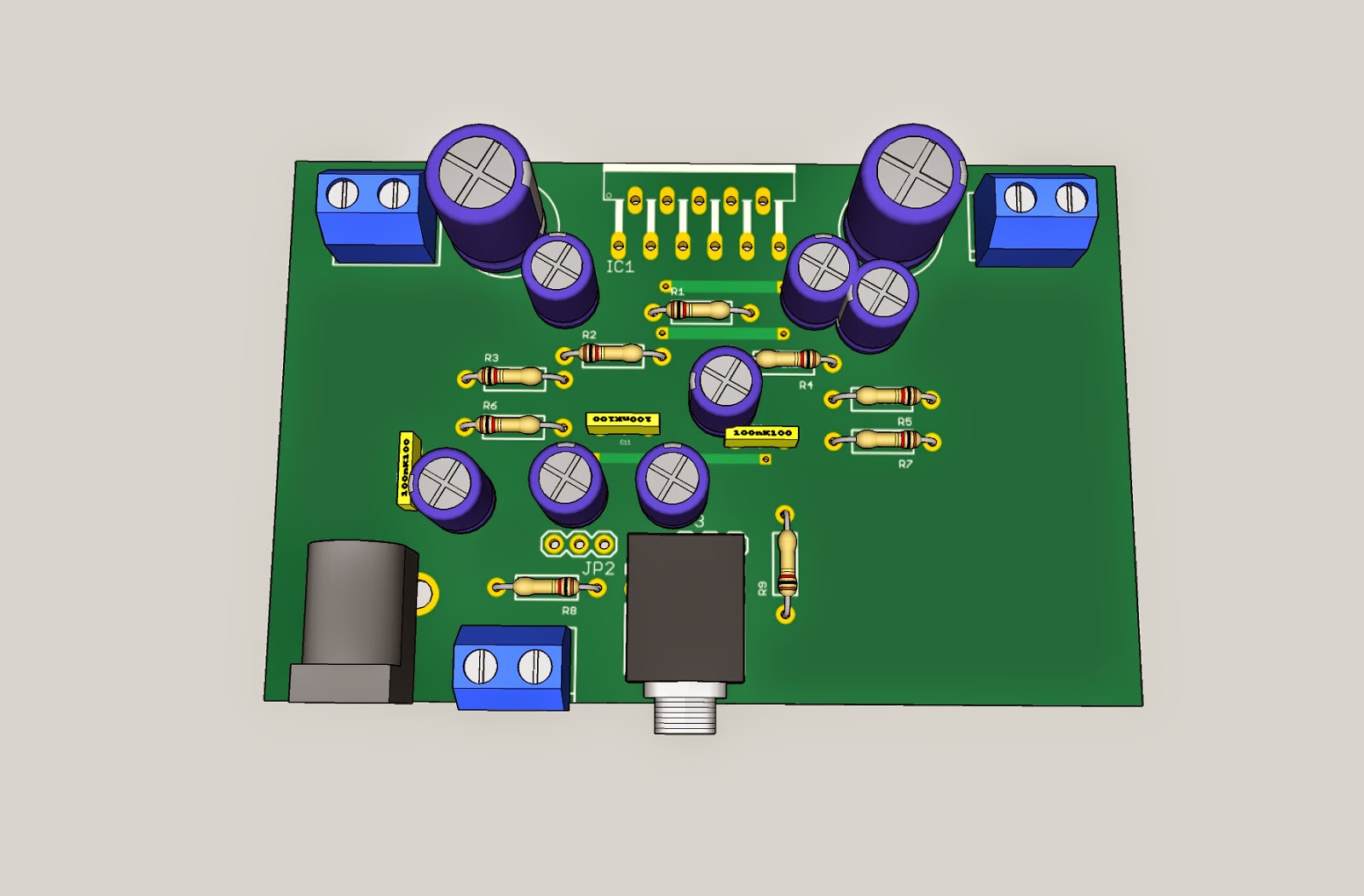
Here are some renders of the PCB and what it might look like when populated. I haven't got a model for the TDA2005 so it doesn't show that part:

Here is the proof of function!
That's all for now...Enjoy people and take care - Langster!
The circuit is easy to understand. Most of the work is performed by the circuitry contained within the TDA2005 amplifier. C1 & C2 are input coupling capacitors and block any DC voltage present in the input audio signal. C10 & C11 are also DC blocking capacitors and C7 & C9 block DC voltage from the feed back loop to the differential inputs of the amplifiers. Resistors R3 and R5 (and R4 and R6) set the level of negative feed back. C10 and R7 (and C11 and R8) provide a high frequency load for stability where the loudspeaker's inductive reactance may become excessive. C4 and C5 provide power supply decoupling or filtering.
The gain is set by the formula 1 + (R3/R5). So in the case of the above circuit it is:
Av = 1 + (1200 / 33)
Av = 37.36
The gain may be increased by reducing the feedback resistors R5 and R6. A value of 22 ohms would provide a gain of approximately 55. If you need much more than 60x gain, it would be better to use a preamplifier such as the LM386 Ruby amplifier circuit and then amplify it.
The maximum supply voltage for this Kit is 18V and the minimum current is 2A. Check the power supply voltage and current and check the polarity before turning the amplifier on.
Unfortunately there is no spice model available for the TDA2005 circuit so I cannot provide a simulation. I have not actually built the circuit yet so I also cannot provide a video of it in operation. I have ordered the components however and as soon as I make a PCB I will populate it and post a video of it working. Here is the PCB layout top and bottom layers:
 |
| PCB Top Layer with components |
 |
| PCB Bottom Layer |
Part |
Value | Description |
| C1 | 2.2uF | 16V Electrolytic Capacitor |
| C2 | 2.2uF | 16V Electrolytic Capacitor |
| C3 | 10uF | 16V Electrolytic Capacitor |
| C4 | 100uF | 16V Electrolytic Capacitor |
| C5 | 100uF | 16V Electrolytic Capacitor |
| C6 | 220uF | 16V Electrolytic Capacitor |
| C7 | 220uF | 16V Electrolytic Capacitor |
| C8 | 2200uF | 16V Electrolytic Capacitor |
| C9 | 2200uF | 16V Electrolytic Capacitor |
| C10 | 100nF | 50V Ceramic Capacitor |
| C11 | 100nF | 50V Ceramic Capacitor |
| C12 | 100nF | 50V Ceramic Capacitor |
| IC1 | TDA2005T | Stereo 10W Power OP AMP |
| J1 | POWER_JACKPTH | DC Power Jack |
| JP1 | Audio Input | 3.5mm Audio Jack |
| JP2 | Dual Gang Potentiometer | 10k Dual Gang Pot |
| JP3 | Dual Gang Potentiometer | 10k Dual Gang Pot |
| JP4 | Speaker Terminals | 5mm Screw Terminal |
| JP5 | Speaker Terminals | 5mm Screw Terminal |
| JP6 | Alternative DC power input | 5mm Screw Terminal |
| R1 | 120k | 1/4W 5% Carbon Film Resistor |
| R2 | 1.2k | 1/4W 5% Carbon Film Resistor |
| R3 | 33R | 1/4W 5% Carbon Film Resistor |
| R4 | 1.2k | 1/4W 5% Carbon Film Resistor |
| R5 | 33R | 1/4W 5% Carbon Film Resistor |
| R6 | 1R | 1/4W 5% Carbon Film Resistor |
| R7 | 1R | 1/4W 5% Carbon Film Resistor |
| R8 | 1k | 1/4W 5% Carbon Film Resistor |
| R9 | 1k | 1/4W 5% Carbon Film Resistor |
| PCB | PCB to mount components on | |
| Heatsink | Heatsink for TDA2005 |
Here are some renders of the PCB and what it might look like when populated. I haven't got a model for the TDA2005 so it doesn't show that part:


The maximum amount of output from the amplifier depends upon the supply voltage, current and speaker impedance. In order to get 10 Watts on each channel the designer must ensure a supply capable of 15 Volts and 2 Amps and a speaker impedance of 1.6 Ohms. A higher speaker impedance will cause the amplifier to draw more power and not output 10 Watts. I reckon I'm getting 6 Watts per channel which is more than acceptable for my purposes....
Here are the Eagle design files if people wish to make their own:
This comment has been removed by a blog administrator.
ReplyDeleteAwesome!
ReplyDeleteIncreasing the C8 and C9 capacitance should, in theory, improve the bass response. It would take up more space, but something to consider.
I agree!
DeleteI haven't done anything with this amplifier for some time - increasing the C8 and C9 caps will probably improve bass response. Are you looking to build this circuit or just browsing? Eaither way thank you for reading and commenting on by blog!
Hello, I love reading your blog. It is really very impressive. I want to leave a comment in your support. Carry on with good continuation. Best of luck for your blogging efforts.
ReplyDelete