Elbert V2 VHDL Tutorial
Now we are going to learn how to use and apply logical operators to the switch actions so that the LEDs only come on (Go High) when two buttons are pressed together (AND) function and when on a different pair of buttons if either button is pressed an LED illuminates (OR) Function. We have already used the invert or NOT function so this shouldn't be too hard!
Here is the code solution from the previous tutorial:
1 2 3 4 5 6 7 8 9 10 11 12 13 14 15 16 17 18 19 20 21 22 23 24 25 | library IEEE; use IEEE.STD_LOGIC_1164.ALL; entity Switch_LEDS is Port ( Switch_One : in STD_LOGIC; Switch_Two : in STD_LOGIC; LED_One : out STD_LOGIC; LED_Two : out STD_LOGIC; Seven_Segment_Transistor_One : out STD_LOGIC; Seven_Segment_Transistor_Two : out STD_LOGIC; Seven_Segment_Transistor_Three : out STD_LOGIC); end Switch_LEDS; architecture Behavioral of Switch_LEDS is begin LED_One <= NOT Switch_One; LED_Two <= NOT Switch_Two; Seven_Segment_Transistor_One <= '1'; --Turn PNP transistor off Seven_Segment_Transistor_Two <= '1'; --Turn PNP transistor off Seven_Segment_Transistor_Three <='1'; --Turn PNP transistor off end Behavioral; |
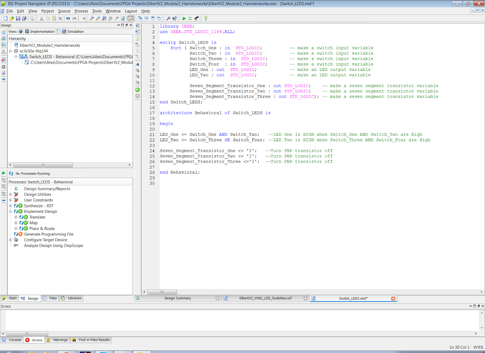
Switch_Three  :  in   STD_LOGIC;    -- make a switch input object
Switch_Four   :  in   STD_LOGIC;    -- make a switch input object
The lines above need to be inserted into the 'entity function' between the inputs and outputs on line 7:
1 2 3 4 5 6 7 8 9 10 11 12 13 14 15 16 17 18 19 20 21 22 23 24 25 26 27 28 | library IEEE; use IEEE.STD_LOGIC_1164.ALL; entity Switch_LEDS is Port ( Switch_One : in STD_LOGIC; -- make a switch input variable Switch_Two : in STD_LOGIC; -- make a switch input variable Switch_Three : in STD_LOGIC; -- make a switch input variable Switch_Four : in STD_LOGIC; -- make a switch input variable LED_One : out STD_LOGIC; -- make an LED output variable LED_Two : out STD_LOGIC; -- make an LED output variable Seven_Segment_Transistor_One : out STD_LOGIC; -- make a seven segment transistor variable Seven_Segment_Transistor_Two : out STD_LOGIC; -- make a seven segment transistor variable Seven_Segment_Transistor_Three : out STD_LOGIC); -- make a seven segment transistor variable end Switch_LEDS; architecture Behavioral of Switch_LEDS is begin LED_One <= NOT Switch_One; -- LED one state is the opposite of the switch one state LED_Two <= NOT Switch_Two; -- LED two state is the opposite of the switch two state Seven_Segment_Transistor_One <= '1'; --Turn PNP transistor off Seven_Segment_Transistor_Two <= '1'; --Turn PNP transistor off Seven_Segment_Transistor_Three <='1'; --Turn PNP transistor off end Behavioral; |
What we need to do now is change the behavior of the program in 'architecture' section to make the first LED come on when switches one and two are pressed at the same time (AND function) and make the second LED come on when either switch three or four is pressed (OR function).
This isn't that hard....helpfully VHDL has the AND and OR functions built in. All we need to do is use the correct assignment syntax and our program will work.
LED_One <= Switch_One AND Switch_Two;
LED_Two <= Switch_Three OR Switch_Four;If we add the above two lines to the architecture section the job is done! I have noticed that the Elbert V2 board is active low and therefore needs inverting to ensure the LEDS are off to begin with. We therefore need to invert the logic to make the LED off to begin. Here is the complete code:
1 2 3 4 5 6 7 8 9 10 11 12 13 14 15 16 17 18 19 20 21 22 23 24 25 26 27 28 | library IEEE; use IEEE.STD_LOGIC_1164.ALL; entity Switch_LEDS is Port ( Switch_One : in STD_LOGIC; -- make a switch input variable Switch_Two : in STD_LOGIC; -- make a switch input variable Switch_Three : in STD_LOGIC; -- make a switch input variable Switch_Four : in STD_LOGIC; -- make a switch input variable LED_One : out STD_LOGIC; -- make an LED output variable LED_Two : out STD_LOGIC; -- make an LED output variable Seven_Segment_Transistor_One : out STD_LOGIC; -- make a seven segment transistor variable Seven_Segment_Transistor_Two : out STD_LOGIC; -- make a seven segment transistor variable Seven_Segment_Transistor_Three : out STD_LOGIC); -- make a seven segment transistor variable end Switch_LEDS; architecture Behavioral of Switch_LEDS is begin LED_One <= NOT Switch_One AND NOT Switch_Two; --LED One is HIGH when Switch_One AND Switch_Two are High LED_Two <= NOT Switch_Three OR NOT Switch_Four; --LED Two is HIGH when Switch_Three AND Switch_Four are High Seven_Segment_Transistor_One <= '1'; --Turn PNP transistor off Seven_Segment_Transistor_Two <= '1'; --Turn PNP transistor off Seven_Segment_Transistor_Three <='1'; --Turn PNP transistor off end Behavioral; |
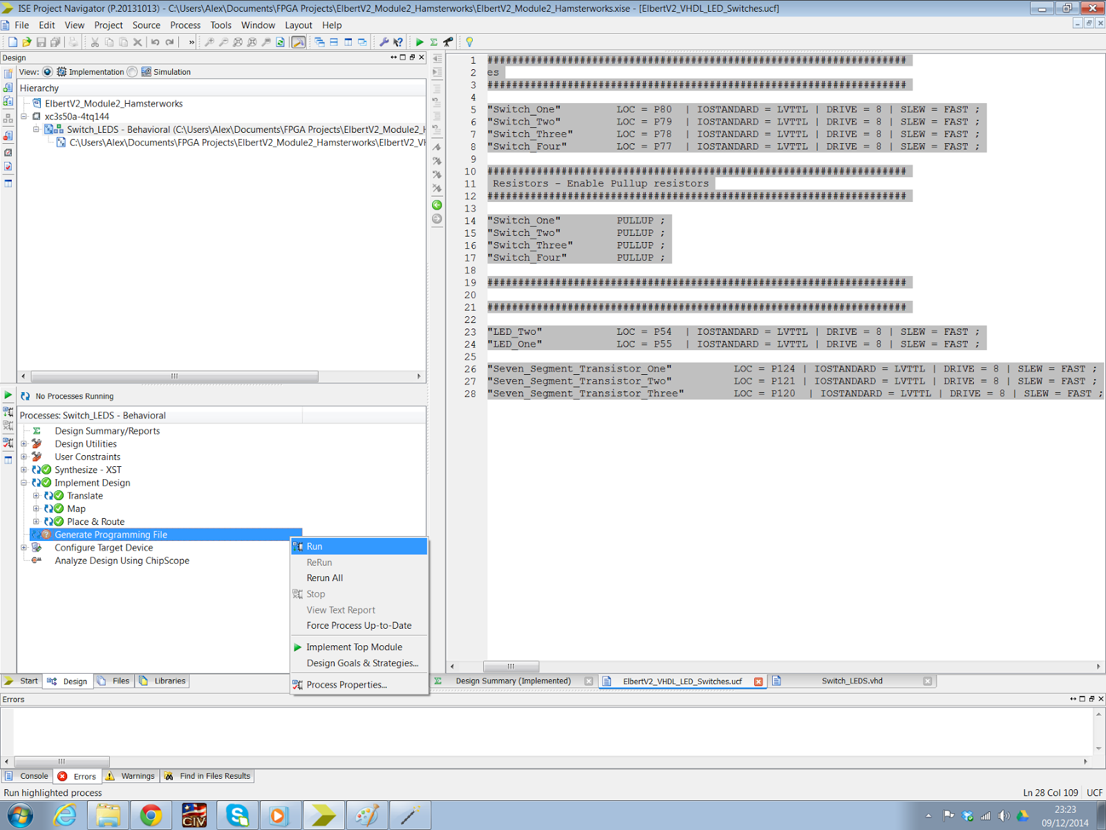
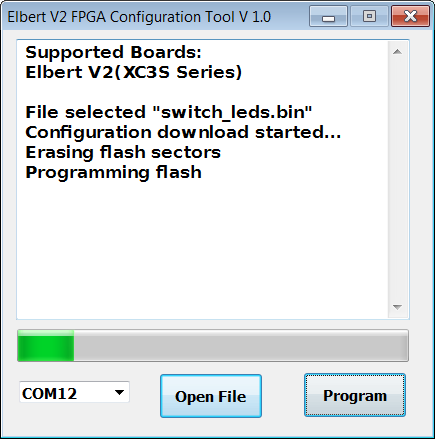
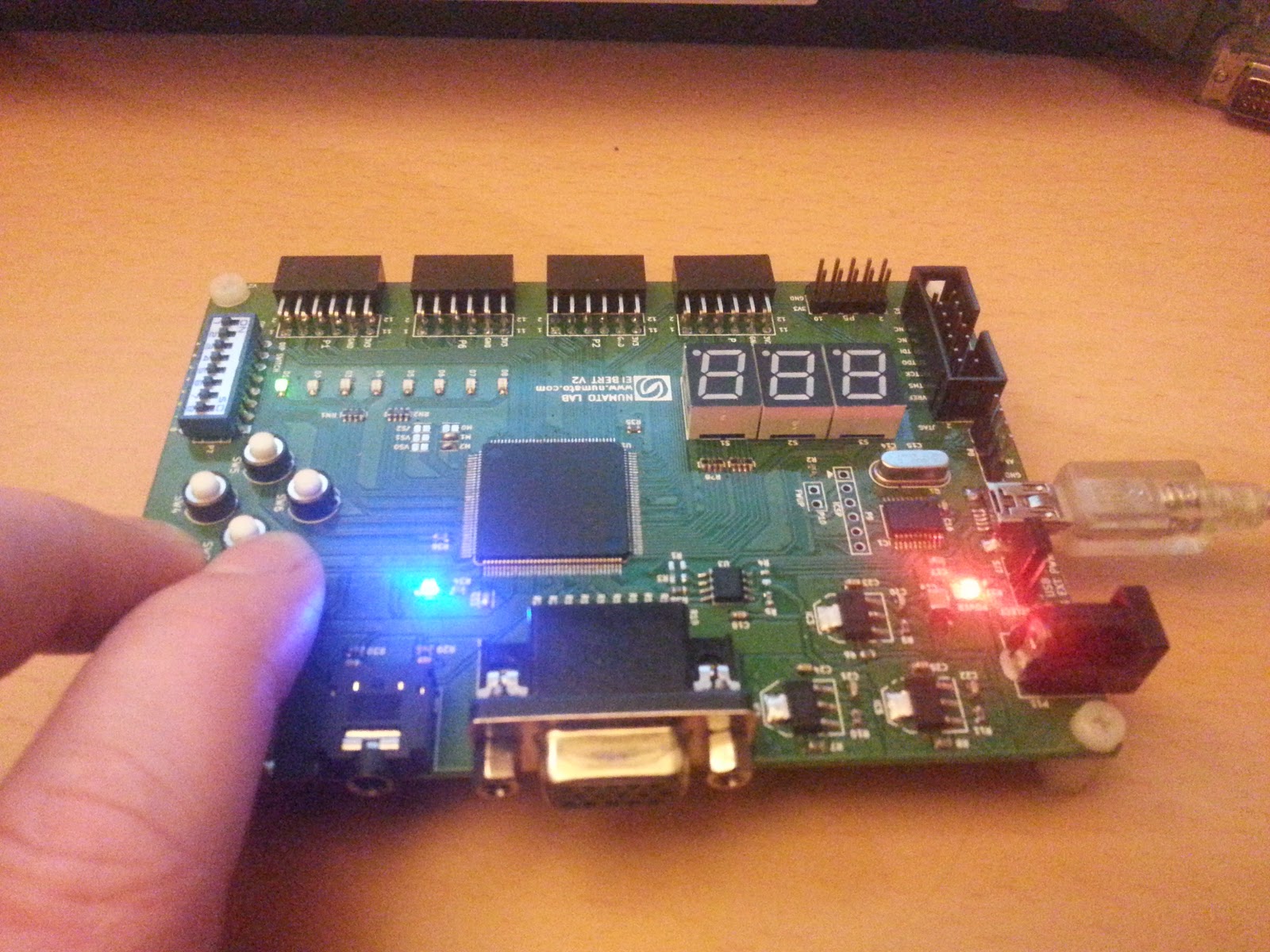
Lets load up ISE Project navigator and update the code for the Switch LED tutorial. We need to open the project and then load the Switch_LEDS behavioral file in the inbuilt text editor and copy and paste the above code:Next we need to 'recompile' the project to ensure there are no issues present - Click on the implement top level arrow. It will prompt you to save the behaviour file if you haven't already and then it will 'recompile' the implementation.Once that's complete we need to update the user constraints file to reflect that we now have two extra switches in the project. Which pins on the FPGA are these switches connected to and also turn on the internal pullup resistors. To do that we need to consult the schematic diagram for the Elbert V2 Development board:Switch three is connected to pin 78 and switch four is connected to pin 77. Load up the implementation constraints file in Xilinx project navigator and update the code - Here is the updated 'UCF file' code:############################################################################ # Switches ############################################################################ NET "Switch_One" LOC = P80 | IOSTANDARD = LVTTL | DRIVE = 8 | SLEW = FAST ; NET "Switch_Two" LOC = P79 | IOSTANDARD = LVTTL | DRIVE = 8 | SLEW = FAST ; NET "Switch_Three" LOC = P78 | IOSTANDARD = LVTTL | DRIVE = 8 | SLEW = FAST ; NET "Switch_Four" LOC = P77 | IOSTANDARD = LVTTL | DRIVE = 8 | SLEW = FAST ; ############################################################################ # PULLUP Resistors - Enable Pullup resistors ############################################################################ NET "Switch_One" PULLUP ; NET "Switch_Two" PULLUP ; NET "Switch_Three" PULLUP ; NET "Switch_Four" PULLUP ; ############################################################################ # LED ############################################################################ NET "LED_Two" LOC = P54 | IOSTANDARD = LVTTL | DRIVE = 8 | SLEW = FAST ; NET "LED_One" LOC = P55 | IOSTANDARD = LVTTL | DRIVE = 8 | SLEW = FAST ; NET "Seven_Segment_Transistor_One" LOC = P124 | IOSTANDARD = LVTTL | DRIVE = 8 | SLEW = FAST ; NET "Seven_Segment_Transistor_Two" LOC = P121 | IOSTANDARD = LVTTL | DRIVE = 8 | SLEW = FAST ; NET "Seven_Segment_Transistor_Three" LOC = P120 | IOSTANDARD = LVTTL | DRIVE = | SLEW = FAST ;Save the file and then its time to generate a 'Binary Configuration File' by clicking on the appropriate button in ISE Project Navigator:Once that has completed connect up the Elbert V2 development board to your PC via a USB cable and load up the programming software. Select the appropriate COM port. Now its time to load up the .BIN file we just created and program the FPGA.Once programming is complete press some buttons! What you should find is that LED 1 only goes 'ON' when both switch 1 and switch 2 are pressed. LED 2 only goes 'ON' when either switch 3 or switch 4 are pressed! Good luck!That's all for now - take care,Langster!

No comments :
Post a Comment