How to input a schematic diagram using Eagle
Load up Eagle 7.1 and load up the light dark detector project
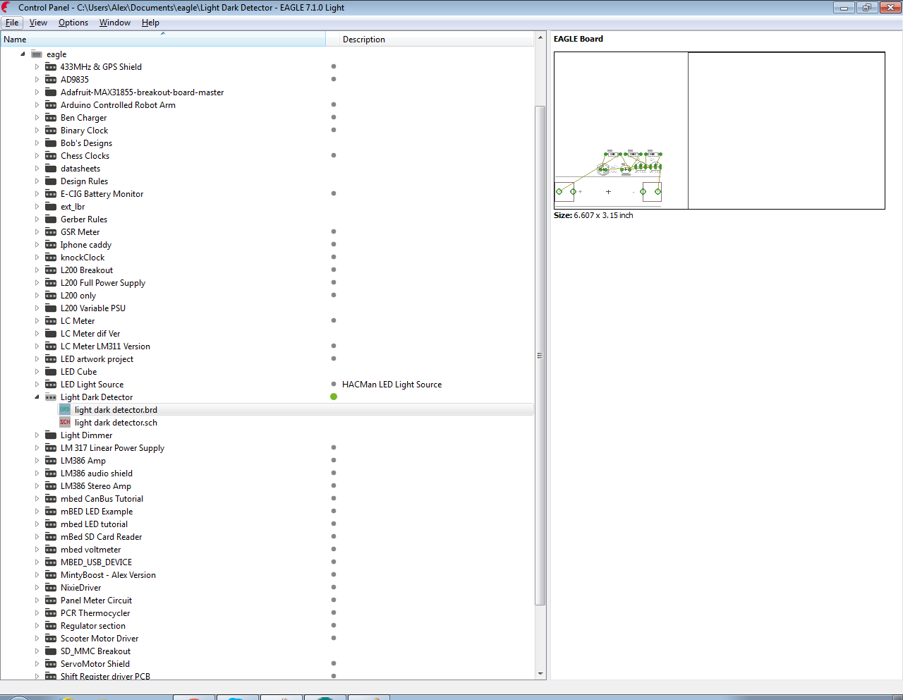
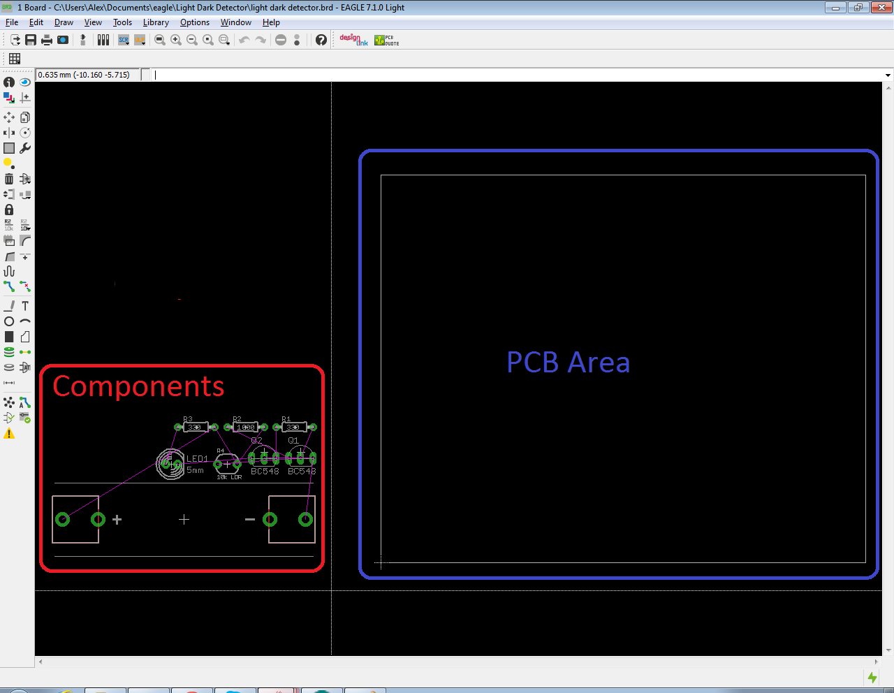
The PCB layout window will be displayed:

The PCB size and the components we chose from the schematic are displayed. Before we begin placing the components onto the PCB and connecting tracks lets make the display easier to use and see.
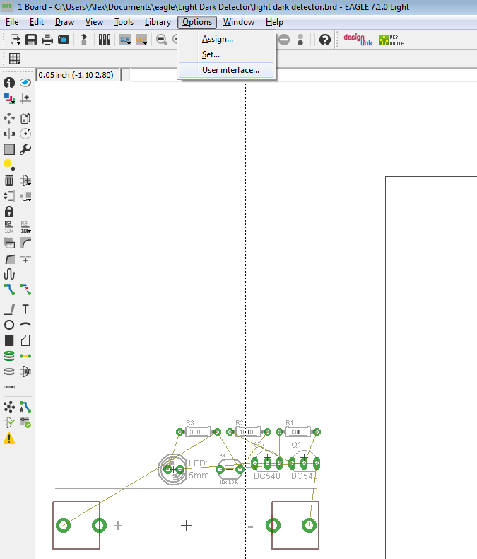
I prefer when laying out a PCB to have a black background, it's easier on the eyes. Click on the user menu at the top of the display and then on the 'User Interface' option.
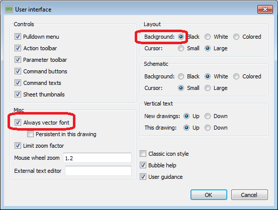
Another window will be displayed providing various options. Click on the radio button to select a black background and I also selected always vector font. Then click the 'Ok' button:
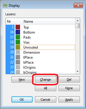
Next lets make the connections between the components easier to see. These are known as 'Airwires'. So called as they show that the components are to be connected together but are not connected by a conductive track but by 'Air'. Click on the layers icon on the toolbar on the left and navigate to 'Unrouted' - layer 19 which is currently a gold colour.

Click on the 'Change' button and change it to something bright and distinctive - I use bright pink!
Click the 'Ok' button when finished. The last thing I tend to do when designing a PCB is apply a grid to the screen so that I know roughly how far apart components are and that the connections 'snap' to the components easily. Click on the 'View' menu and select 'Grid':

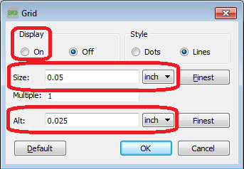
We are going to change the scale from imperial (inches) to metric and then change the size of the grid to 0.635mm for normal squares and 0.3125 for the alternative size. Finally click on the 'Display' radio button to 'On'.

Click on the 'Ok' button to apply the settings. The reason for applying the above grid settings is that firstly I have more of an appreciation for metric units and mm - you can use inches if that suits you. I chose the grid sizes as these are commonly used and apply to most components. The pitch (space between the legs) of most components is 0.1 inches which is 1.27mm, I'm using a grid of half of that and half again as an alternative. This means when we draw the lines for the tracks the pins from the components will immediately line up with the tracks.
The grid pattern cannot currently be seen as there is another setting that needs to be changed in order to make the grid visible. Click on the 'Options' menu again and navigate to 'Set'. A new window will be displayed, click on the black box relating to the colour of the grid when using a black background and choose something brighter. I use a light grey. Click on 'Ok' when ready to return to the main PCB editor window. When you zoom in the grid should be visible, you can use the mouse wheel to zoom in and out.

We are now ready to start designing the PCB. This is where we will arrange the components to suit our purposes, connect the tracks between them, decide the final size of the PCB and arrange the labelling so we know where to place each component and in what orientation. This way populating the PCB will be very easy.
There are no hard and fast rules on PCB layout and design. It is what suits your purposes and your specific situation. Most designers decide to use the smallest most efficient layout. Hopefully this means that the PCB is easy to make, populate and fit in a suitable enclosure (case). It isn't always easy and there are often decisions to make which affect how the layout will proceed. As there are not too many components in this example it won't be too difficult to do. When there are more than 100 components it becomes much more complex and that is why a lot of electronics engineers will say that PCB layout is an much art as engineering. I agree to a point....I always just make my designs work first and then apply the 'art' afterwards! I don't consider myself to be particularly artistic however...
We are going to manually place the components on the PCB and then rotate them to suit before connecting tracks between them. This is known as manually routing, when designs get more complicated there are special functions within PCB design software to make it easier for the design engineer. The most common one that is discussed is the 'autorouter' function. I'm going to discuss autorouting in another post.
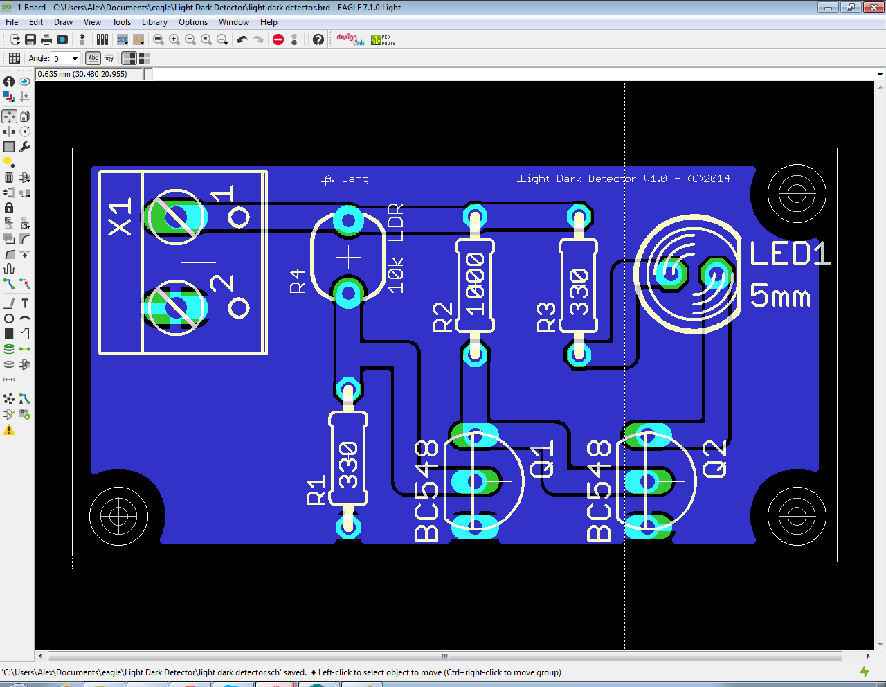
The screenshot below should should match what you have on your screen - not including the text or coloured rings:
If we zoom in and look at the components we see the outlines of the packages of the components with some green circles. These are the component 'footprints' we selected when the schematic was drawn. The green circles are the holes the component legs will go through when the PCB is to be populated. Press 'Alt +F2' in order to zoom out but fit all items to the screen.

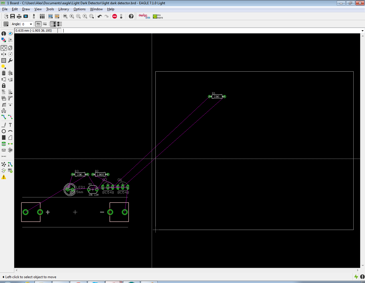
In order to start the layout we need to move the components onto the PCB. Left Click on the move icon in the tool bar and then left click on the resistor component R1:

This will select the component and then when you move the mouse pointer the component will move with it. Place the resistor component onto the PCB area:
Repeat this process for all of the components, once complete you should see something similar to the screen below. I turned the grid off to make things easier to see....

At this point I like to refer to the schematic diagram. It makes it easier to see which components are connected together and in which order. As I have said before there are no rules when designing a PCB. The decisions are all in the designers hands and mind. I like to start with the power supply section of the circuit which in this case is the battery. With the move icon selected - Click on the battery component and move it to the bottom left corner of the PCB. Next right click the mouse button - this rotates the component. Rotate the component until the positive connection is at the top and the entire component sits in the bottom left corner:

Next lets move and orientate the LDR component. We want to place it somewhere sensible so that the light can shine on it but also in such a way that it is easy to connect to the positive terminal of the battery. With the 'move' icon selected click on the LDR component and move it and orientate it so that it is easy to connect to the battery positive terminal:
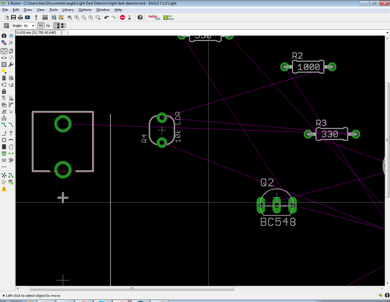
Now it is time to move the R1 component (330 Ohm resistor) to somewhere on the PCB that makes it easy to connect to the LDR and the 0V connection of the battery. I put mine directly below the LDR but it could go anywhere as long as it is easy to connect the tracks and place the components without difficulty.

You may notice that there are lots of purple lines crossing the screen connecting the components in some sort of random pattern. These are the unrouted 'Air wires' discussed earlier. If you find the air wires annoying you can turn them off or have Eagle re-calculate them. To turn them off click on the layers icon as before and navigate to layer 19 and unselect it. To have Eagle re-calculate their path click on the 'Rats Nest' Icon on the bottom of the toolbar on the left side of the screen:

It will change the purple airwires to and calculate the shortest path for components to connect to each other. Move all of the rest of the components, using the schematic as a reference, until all of the airwires are easy to follow and do not cross each other. This is possible on simple designs like this but not always. I often click the 'ratsnest' icon when moving and placing components. Again there is no correct or incorrect way to place components. Choose the most logical way to do it, rotate the components every which way until the airwires don't cross and there is a sensible amount of space between each component:
Hopefully your screen should look something similar to the screen above. Now it is time to draw tracks between the components to connect them together. Click on the 'Route manually' Icon and then click on the width drop down menu in top middle toolbar; we are going to select the track width.

I chose 1.27 mm as this means that the tracks are the same size as most of the components pads. The tracks don't have to be this thick. They need to be thick enough to carry the current flowing through them (18 mA). There are online calculators for working out the current carrying capacity of PCB tracks however as a rule of thumb anything thicker than 0.5mm will be capable of carrying 100 mA without getting hot. The thicker the track the more current carrying capacity and the easier it is to make the PCB.
Left click on the top pad of the battery - the pad will be highlighted and when you move the mouse a blue line will be drawn, this is the PCB track. The pad the track has to connect to (the LDR) will also be highlighted. Move the mouse until the track covers the top pad on the LDR and then left click the mouse. Congratulations you have just make your first PCB track connection. This track is on the underside of the PCB (bottom layer). If you wanted to place a track on the top layer then click on the layer icon on the top toolbar (highlighted) and then place a track as before. It will be red in colour to show that the track is on the top layer. If you want to remove a track click on the icon next to the route manually icon which is called 'Ripup'. Then click on the track you would like to remove.

For this design there is no need to route tracks on both layers so I will be making this PCB single sided. However for more complex designs it is often necessary to route tracks on several layers and interconnect them using 'vias' - special connections which join the routed tracks together. You may also notice I have turned the grid back on. I find it easy to route tracks with the grid on.
Now lets route all of the other tracks...its the same process as before. Once complete it should look something like this:

Technically we could save here...generate the 'gerber' files and get a PCB made however we are wasting a lot of space on the PCB. Anywhere we we can see black we are wasting valuable space or 'real estate' as it is sometimes referred to. Lets stop wasting real estate and change our PCB dimensions. Left click on the 'move' icon and then click on the external PCB dimensions (white rectangle) and resize it:

I turned the grid off for the resizing as I found it hard to see what I was doing.
I don't like the footprint for the battery connector. I never intended using one single AA battery to power the circuit which wouldn't work anyway. I intended to solder some wires from a battery connector to two pads on the circuit board. Lets change the package for the battery to something more suitable. Right click on the battery footprint and select 'Replace'
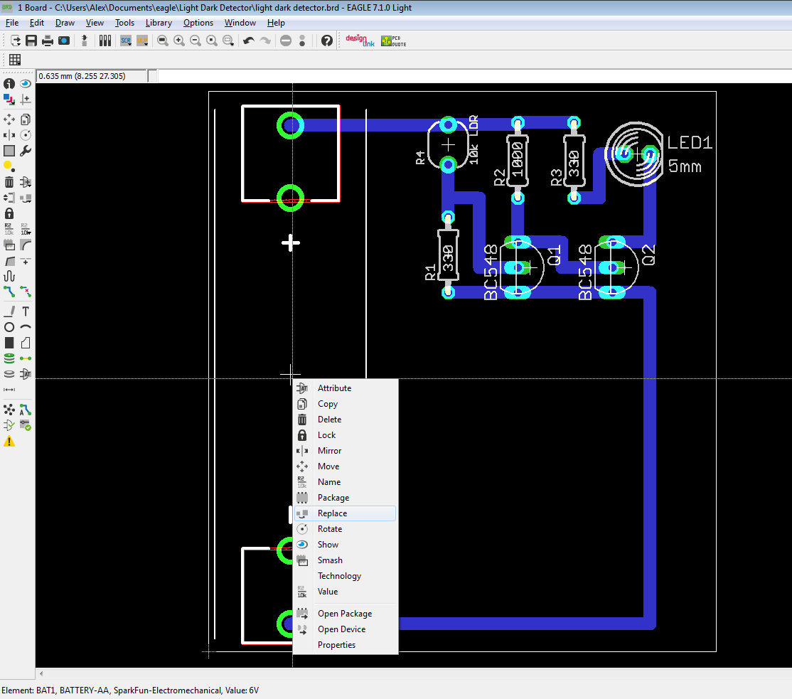
The replace window will be displayed. We need to search for a footprint that has two pads that is reasonably small and suitable for our purposes. There are several to choose from. I like to use screw connectors for this purpose. Type 'screw' in the search box and see what appears:
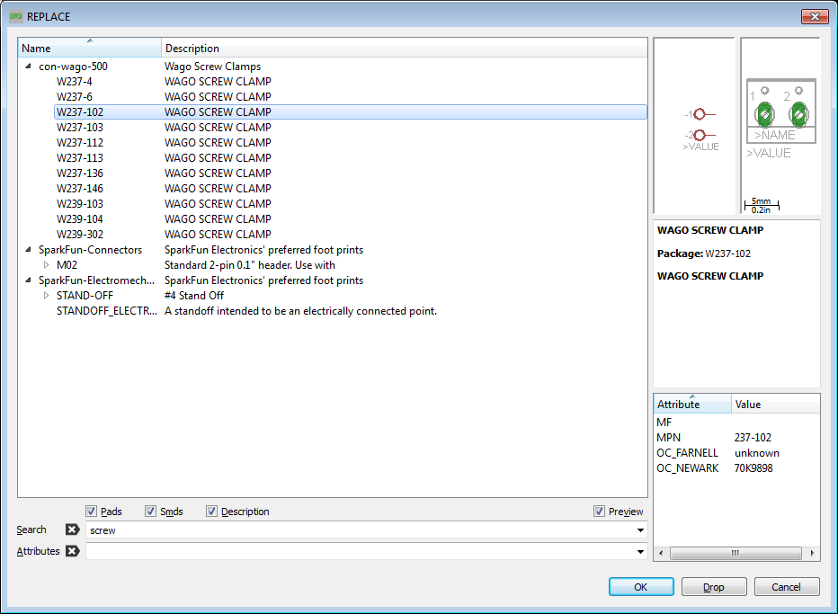
These are all of the packages with the word 'screw' in their description. I'm going to select the one highlighted. It's a two terminal through hole screw terminal from Wago. Any two terminal connector would do however. Click 'Ok' to replace the battery terminal. Unfortunately when you do this an error message is displayed:

This is because the symbol used in the schematic cannot be related to the new package we selected. In order to solve this problem we need to edit our schematic diagram. We need to switch back to the schematic editor and change the symbol there. Click on the 'switch to board' icon to return to the schematic editor:
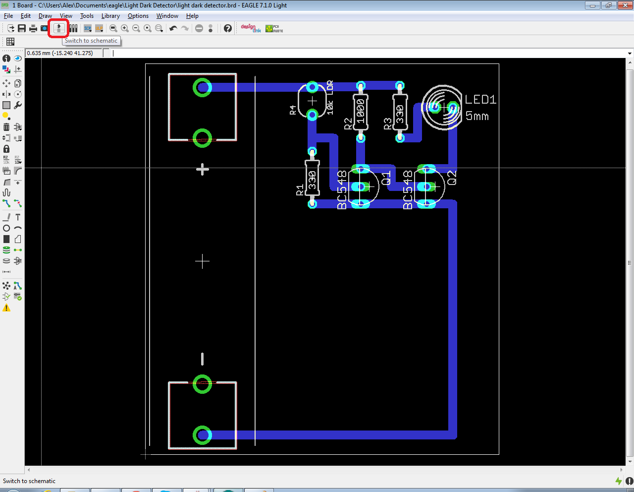
In the schematic editor delete the battery symbol by clicking on the trashcan icon in the left toolbar, Then click on the battery symbol.

Next click on the 'Add' Icon and search for 'Screw' - select the wago screw terminal seen previously and place it on the schematic in the same place that the battery symbol was:

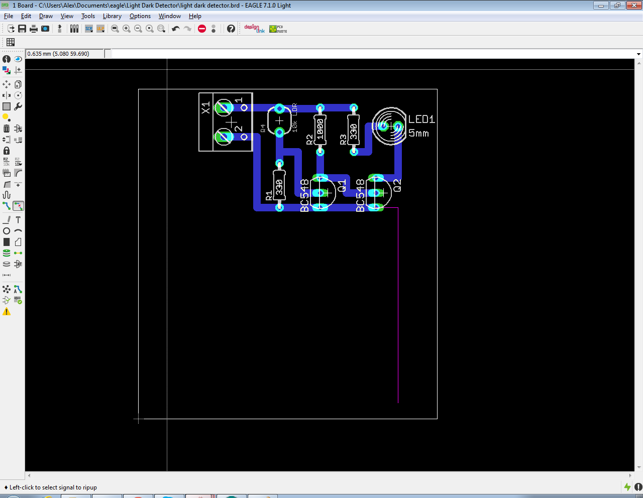
Switch back to the PCB editor and you can now see the screw terminal connector:

Click on the 'Move' Icon and then place the screw terminal package somewhere sensible next to R1 and the LDR. After that click on the 'Route Manually' button and connect the tracks. Remove any unwanted tracks using the 'Ripup' tool.
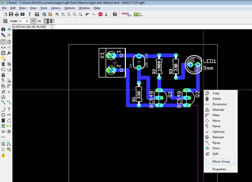
Now we should probably move all of the components and tracks to the bottom left of the PCB and then resize it as we still have a lot of unused 'real estate'. Click on the 'Move' Icon and then click on the 'Group' Icon. Now Left click and drag a box around all of the components and tracks and the release the left mouse button:

The 'Move' icon will immediately be select as it was the previous tool used. Right click on the components and select 'Move Group' and then move the components and tracks to the bottom left corner of the PCB.
Now lets resize the PCB to save on space and not waste 'real estate':

Now is probably a good time to save your work. I tend to save my work as often as I can as I hate having to repeat things. Other than that we should probably add some mounting holes. Click on the 'Holes' tool and select a 3.2mm hole:

Click and place holes on the layout. These holes are for mounting to. I'm going with three separate holes in corners:

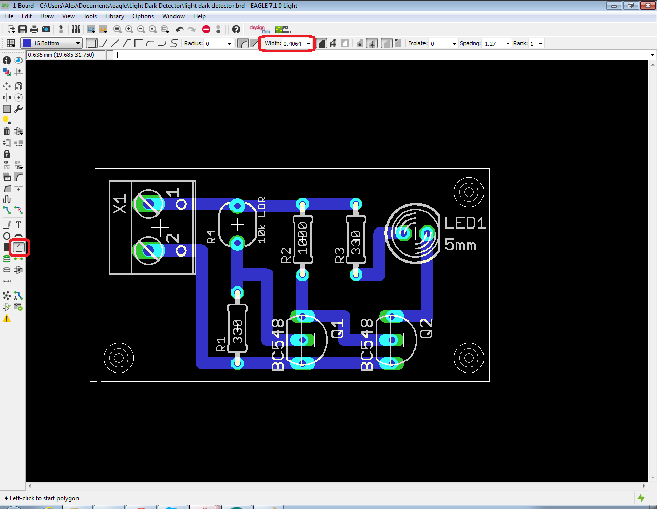
Then click and draw a square around the outside edge of the PCB:
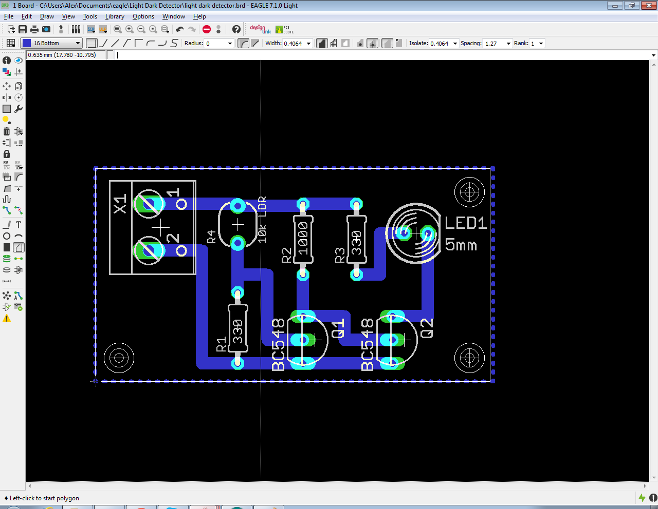
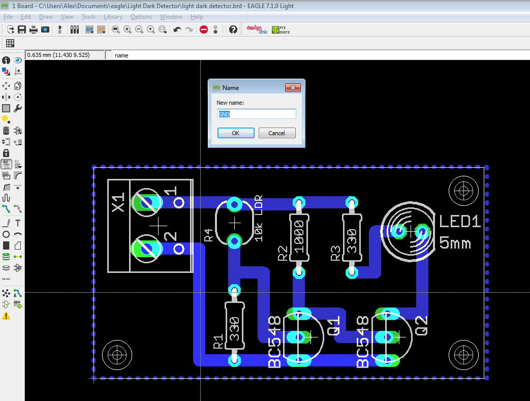
Click on the Command field and type 'name' and press 'enter':

Next click on the lower track connected to the screw connector and R1. A window will appear. Type GND into the box and click 'Ok'. This changes the net name of the track to GND. Now click on the dashed outline of the polygon for the ground plane and call that GND also. This will connect the polygon to the track.
To complete the process click on the 'Ratsnest' tool. This will display the ground plane:

I would now consider the PCB layout complete however we should probably add a label or two. It is always a good idea to label the PCB so we know what it is and like any good artist we should sign our work! Click on the 'Text' tool in the left toolbar and add a name to the PCB along with a description:

Place the labels somewhere suitable (where there is space) but not on the PCB. The label will be oversized and on the wrong layer at the moment. Click on the 'Info' Icon and then set the size, font and layer and unclick the mirror checkbox as shown in the image below,:
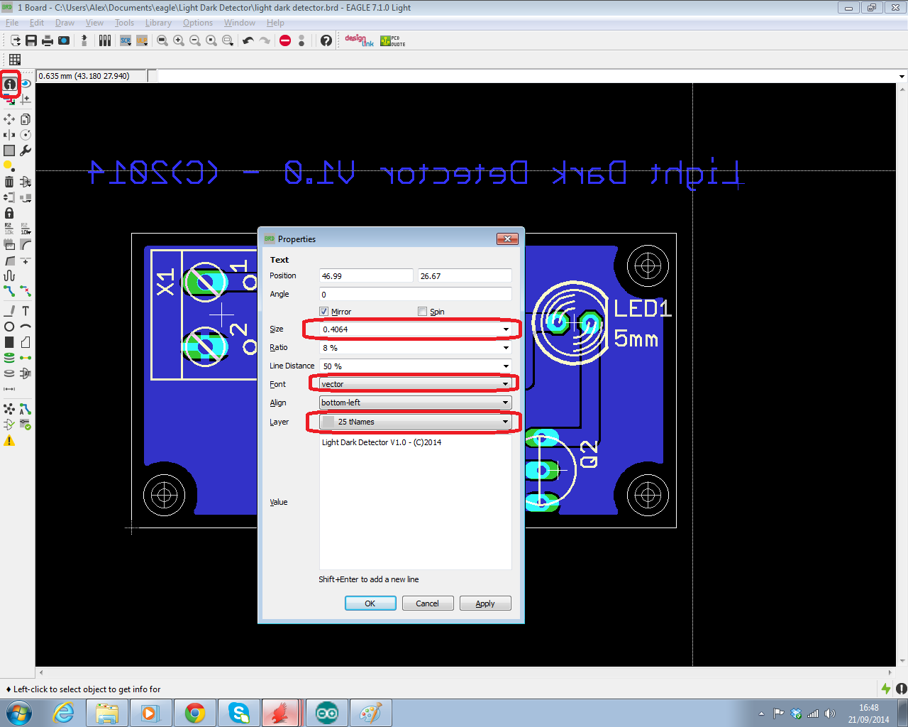
This should resize the label so you can then place it somewhere suitable on the PCB:
Save your work and take a break. That is the PCB design complete! The next post will discuss preparing a design for professional manufacture and creating an enclosure.
If you want to make a home made version of your design then the following previous post might be of interest:
How to make a PCB
That's all for now - take care, Langster!
This comment has been removed by a blog administrator.
ReplyDeleteThis comment has been removed by a blog administrator.
ReplyDeleteWonderful work! This is the kind of info that are meant to be shared across the internet. Disgrace on the search engines for not positioning this post higher! Come on over and consult with my website.
ReplyDeleteSo, I would like to Share FlixGrab Premium Crack with you.
WordWeb Pro Crack
"PCB Manufacturer - Online PCB Board Design | PCB Power Market
ReplyDelete"